Bank switching

Bank switching is a technique used in computer design to increase the amount of usable memory beyond the amount directly addressable by the processor[1] instructions. It can be used to configure a system differently at different times; for example, a ROM required to start a system from diskette could be switched out when no longer needed. In video game systems, bank switching allowed larger games to be developed for play on existing consoles.
Bank switching originated in minicomputer systems.[2] Many modern microcontrollers and microprocessors use bank switching to manage random-access memory, non-volatile memory, input-output devices and system management registers in small embedded systems. The technique was common in 8-bit microcomputer systems. Bank-switching may also be used to work around limitations in address bus width, where some hardware constraint prevents straightforward addition of more address lines, and to work around limitations in the ISA, where the addresses generated are narrower than the address bus width. Some control-oriented microprocessors use a bank-switching technique to access internal I/O and control registers, which limits the number of register address bits that must be used in every instruction.
Unlike memory management by paging, data is not exchanged with a mass storage device like disk storage. Data remains in quiescent storage in a memory area that is not currently accessible to the processor (although it may be accessible to the video display, DMA controller, or other subsystems of the computer) without the use of special prefix instructions.
Technique
Bank switching can be considered as a way of extending the address space of processor instructions with some register. Examples:
- The original CDC 160 processor has 12-bit addresses; the follow-up CDC 160-A processor, a follow-on to the CDC 160, has a 15-bit address bus, but there is no way to directly specify the high three bits on the address bus. Internal bank registers can be used to provide those bits.[3]
- The CDC 1604 has 15-bit addresses; the follow-on CDC 3600 system has an 18-bit address bus, but legacy instructions only have 15 address bits; internal bank registers can be used to provide those bits. Some new instructions can explicitly specify the bank.[4]
- A processor with a 16-bit external address bus can only address 216 = 65536 memory locations. If an external latch was added to the system, it could be used to control which of two sets of memory devices, each with 65536 addresses, could be accessed. The processor could change which set is in current use by setting or clearing the latch bit.
The latch can be set or cleared by the processor in several ways; a particular memory address may be decoded and used to control the latch, or, in processors with separately-decoded I/O addresses, an output address may be decoded. Several bank-switching control bits could be gathered into a register, approximately doubling the available memory spaces with each additional bit in the register.
Because the external bank-selecting latch (or register) is not directly connected with the program counter of the processor, it does not automatically change state when the program counter overflows; this cannot be detected by the external latch since the program counter is an internal register of the processor. The extra memory is not seamlessly available to programs. Internal registers of the processor remain at their original length, so the processor cannot directly span all of bank-switched memory by, for example, incrementing an internal register.[5] Instead the processor must explicitly do a bank-switching operation to access large memory objects. There are other limitations. Generally[citation needed] a bank-switching system will have one block of program memory that is common to all banks; no matter which bank is currently active, for part of the address space only one set of memory locations will be used. This area would be used to hold code that manages the transitions between banks, and also to process interrupts.
Often a single database spans several banks, and the need arises to move records between banks (as for sorting). If only one bank is accessible at a time, it would be necessary to move each byte twice: first into the common memory area, perform a bank switch to the destination bank, and then actually to move the byte into the destination bank. If the computer architecture has a DMA engine or a second CPU, and its bank access restrictions differ, whichever subsystem can transfer data directly between banks should be used.
Unlike a virtual memory scheme, bank-switching must be explicitly managed by the running program or operating system; the processor hardware cannot automatically detect that data not currently mapped into the active bank is required. The application program must keep track of which memory bank holds a required piece of data, and then call the bank-switching routine to make that bank active.[6] However, bank-switching can access data much faster than, for example, retrieving the data from disk storage.
Microcomputer use

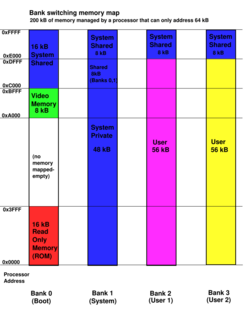
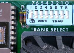
Processors with 16-bit addressing (8080, Z80, 6502, 6809, etc.) commonly used in early video game consoles and home computers can directly address only 64 KB. Systems with more memory had to divide the address space into a number of blocks that could be dynamically mapped into parts of a larger address space. Bank switching was used to achieve this larger address space by organizing memory into separate banks of up to 64 KB each.[8] Blocks of various sizes were switched in and out via bank select registers or similar mechanisms. Cromemco was the first microcomputer manufacturer to use bank switching, supporting 8 banks of 64 KB in its systems.[9]
When using bank switching some caution was required in order not to corrupt the handling of subroutine calls, interrupts, the machine stack, and so on. While the contents of memory temporarily switched out from the CPU was inaccessible to the processor, it could be used by other hardware, such as video display, DMA, I/O devices, etc. CP/M-80 3.0 released in 1983 and the Z80-based TRS-80s the Model 4 and Model II supported bank switching to allow use of more than the 64 KB of memory that the 8080 or Z80 processor could address.[10]
Bank switching allowed extra memory and functions to be added to a computer design without the expense and incompatibility of switching to a processor with a wider address bus. For example, the C64 used bank switching to allow for a full 64 KB of RAM and still provide for ROM and memory-mapped I/O as well. The Atari 130XE could allow its two processors (the 6502 and the ANTIC) to access separate RAM banks, allowing programmers to make large playfields and other graphic objects without using up the memory visible to the CPU.
Microcontrollers
Microcontrollers (microprocessors with significant input/output hardware integrated on-chip) may use bank switching, for example, to access multiple configuration registers or on-chip read/write memory. An example is the PIC microcontroller. This allows short instruction words to save space during routine program execution, at the cost of extra instructions required to access relatively infrequently used registers, such as those used for system configuration at start-up.
IBM PC

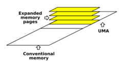
In 1985, the companies Lotus and Intel introduced Expanded Memory Specification (EMS) 3.0 for use in IBM PC compatible computers running MS-DOS. Microsoft joined for versions 3.2 in 1986 and 4.0 in 1987 and the specification became known as Lotus-Intel-Microsoft EMS or LIM EMS.[6][11][12] It is a form of bank switching technique that allows more than the 640 KB of RAM defined by the original IBM PC architecture, by letting it appear piecewise in a 64 KB "window" located in the Upper Memory Area.[13] The 64 KB is divided into four 16 KB "pages" which can each be independently switched. Some computer games made use of this, and though EMS is obsolete, the feature is nowadays emulated by later Microsoft Windows operating systems to provide backwards compatibility with those programs.
The later eXtended Memory Specification (XMS), also now obsolete, is a standard for, in principle, simulating bank switching for memory above 1 MB (called "extended memory"), which is not directly addressable in the Real Mode of x86 processors in which DOS runs. XMS allows extended memory to be copied anywhere in conventional memory, so the boundaries of the "banks" are not fixed, but in every other way it works like the bank switching of EMS, from the perspective of a program that uses it. Later versions of DOS (starting circa version 5.0) included the EMM386 driver, which simulates EMS memory using XMS, allowing programs to use extended memory even if they were written for EMS. Microsoft Windows emulates XMS also, for those programs that require it.
Video game consoles
Bank switching was also used in some video game consoles.[14] The Atari 2600, for instance, had a 12-bit external address space and a 8-bit data bus, so it could only address 212 bytes = 4 KB of ROM,[15][16] so later 2600 game cartridges contained their own bank switching hardware in order to permit the use of more ROM and thus allow for more sophisticated games (via more program code and, equally important, larger amounts of game data such as graphics and different game stages).[17] The Nintendo Entertainment System contained a modified 6502 but its cartridges sometimes contained a megabit or more of ROM, addressed via bank switching called a Multi-Memory Controller. Game Boy cartridges used a chip called MBC (Memory Bank Controller), which not only offered ROM bank switching, but also cartridge SRAM bank switching, and even access to such peripherals as infrared links or rumble motors. Bank switching was still being used on later game systems. Several Sega Mega Drive cartridges, such as Super Street Fighter II were over 4 MB in size and required the use of this technique (4 MB being the maximum address size). The GP2X handheld from Gamepark Holdings uses bank switching in order to control the start address (or memory offset) for the second processor.
Video processing
In some types of computer video displays, the related technique of double buffering may be used to improve video performance. In this case, while the processor is updating the contents of one set of physical memory locations, the video generation hardware is accessing and displaying the contents of a second set. When the processor has completed its update, it can signal to the video display hardware to swap active banks, so that the transition visible on screen is free of artifacts or distortion. In this case, the processor may have access to all the memory at once, but the video display hardware is bank-switched between parts of the video memory. If the two (or more) banks of video memory contain slightly different images, rapidly cycling (page-flipping) between them can create animation or other visual effects that the processor might otherwise be too slow to carry out directly.
Alternative and successor techniques
Bank switching was later supplanted by segmentation in many 16-bit systems, which in turn gave way to paging memory management units. In embedded systems, however, bank switching is still often used for its simplicity, low cost, and often better adaptation to those contexts than to general purpose computing.
See also
- Sideways address space, an example of bank switching on the BBC Micro
- Overlay (programming)
References
- ↑ Aspinall, D., ed (1978). The Microprocessor and its application: an advanced course. CUP Archive. pp. 47–50. ISBN 0-521-22241-9.
- ↑ Computer structures: readings and examples. McGraw Hill. 1971. pp. 156. https://archive.org/details/computerstructur00bellrich.
- ↑ Control Data 160-A Computer Programming Manual. CDC. March 1963. p. 2-09. 145e. https://bitsavers.org/pdf/cdc/160/CDC160A/145e_CDC160A_Programming_Manual_196303.pdf.
- ↑ Control Data 3600 Computer System Reference Manual. CDC. 60021300E. http://bitsavers.org/pdf/cdc/3x00/48bit/3600/60021300E_3600_SysRef_Sep64.pdf.
- ↑ Embedded systems design. Newnes. 2003. pp. 242. ISBN 0-7506-5546-1. https://archive.org/details/embeddedsystemsd00heat.
- ↑ 6.0 6.1 Upgrading and Repairing PCs (2 ed.). Que Books. 1992. pp. 699–700. ISBN 0-88022-856-3. https://archive.org/details/upgradingrepairi0000muel_2ndedition/page/699. Retrieved 2020-02-08.
- ↑ "Design Innovations in Personal Computers". Computer (IEEE Computer Society) 10 (3): 25. March 1977. doi:10.1109/c-m.1977.217669. http://www.computer.org/csdl/mags/co/1977/03/01646402-abs.html. Retrieved 2020-02-08. "An eight-position DIP switch on such cards is used to select one (or more) of eight banks of memory.".
- ↑ Introduction to Microprocessor System Design. McGraw-Hill Book Company. 1979. p. 93. ISBN 0-07-022871-X. https://archive.org/details/introductiontomi00garl/page/93. Retrieved 2020-02-08. "With memory bank select, memory space is arranged in a number of separate banks of up to 64K each."
- ↑ "Share and Share Alike: Multiuser Hardware Explained". InfoWorld 3 (11): 18. 1981-06-08. ISSN 0199-6649. https://books.google.com/books?id=zD0EAAAAMBAJ&pg=PA18. Retrieved 2020-02-08. "Cromemco was the first microcomputer manufacturer to refine and exploit bank switching.".
- ↑ "Digital Research offers CP/M upgrade". InfoWorld 4 (42): 1. 1982-10-25. ISSN 0199-6649. https://books.google.com/books?id=DjAEAAAAMBAJ&pg=PA1.
- ↑ "New 1-2-3 Gets 4 Megabytes of Memory, Lotus, Intel Break PC DOS Memory Barrier". InfoWorld: 15. 1985-04-29. ISSN 0199-6649. https://books.google.com/books?id=2C4EAAAAMBAJ&pg=PA15.
- ↑ Angus, Jeff (1987-08-17). "EMS Update Gives DOS Improved Multitasking". InfoWorld 9 (32): 5. ISSN 0199-6649. https://books.google.com/books?id=2jsEAAAAMBAJ&pg=PA5.
- ↑ Ross, Paul W., ed (1995). The Handbook of Software for Engineers and Scientists. CRC Press. pp. 26. ISBN 0-8493-2530-7.
- ↑ Carey, Charles W., ed (2002). American inventors, entrepreneurs & business visionaries. Infobase Publishing. pp. 322–324. ISBN 0-8160-4559-3. https://archive.org/details/americaninventor00care_0/page/322. Retrieved 2020-02-08.
- ↑ https://grandideastudio.com/media/pp_atari2600_bankswitch_instructions.pdf
- ↑ Atari 2600 Specifications
- ↑ Hardware hacking: have fun while voiding your warranty. Syngress. 2004. pp. 229. ISBN 1-932266-83-6. https://archive.org/details/hardwarehackingh00gran/page/229. Retrieved 2020-02-08.
External links
- "Story about bank switching in the Apple II.". http://www.folklore.org/StoryView.py?project=Macintosh&story=Well_See_About_That.txt.
- "What Is Bank Switching?". 2 February 2024. http://www.wisegeek.com/what-is-bank-switching.htm.
 |
