Engineering:Scanning tunneling microscope
A scanning tunneling microscope (STM) is a type of microscope used for imaging surfaces at the atomic level. Its development in 1981 earned its inventors, Gerd Binnig and Heinrich Rohrer, then at IBM Zürich, the Nobel Prize in Physics in 1986.[1][2][3] STM senses the surface by using an extremely sharp conducting tip that can distinguish features smaller than 0.1 nm with a 0.01 nm (10 pm) depth resolution.[4] This means that individual atoms can routinely be imaged and manipulated. Most scanning tunneling microscopes are built for use in ultra-high vacuum at temperatures approaching absolute zero, but variants exist for studies in air, water and other environments, and for temperatures over 1000 °C.[5][6]
File:Scanning Tunneling Microscope.ogv
STM is based on the concept of quantum tunneling. When the tip is brought very near to the surface to be examined, a bias voltage applied between the two allows electrons to tunnel through the vacuum separating them. The resulting tunneling current is a function of the tip position, applied voltage, and the local density of states (LDOS) of the sample. Information is acquired by monitoring the current as the tip scans across the surface, and is usually displayed in image form.[5]
A refinement of the technique known as scanning tunneling spectroscopy consists of keeping the tip in a constant position above the surface, varying the bias voltage and recording the resultant change in current. Using this technique, the local density of the electronic states can be reconstructed.[7] This is sometimes performed in high magnetic fields and in presence of impurities to infer the properties and interactions of electrons in the studied material.
Scanning tunneling microscopy can be a challenging technique, as it requires extremely clean and stable surfaces, sharp tips, excellent vibration isolation, and sophisticated electronics. Nonetheless, many hobbyists build their own microscopes.[8]
Procedure
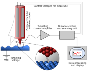
The tip is brought close to the sample by a coarse positioning mechanism that is usually monitored visually. At close range, fine control of the tip position with respect to the sample surface is achieved by piezoelectric scanner tubes whose length can be altered by a control voltage. A bias voltage is applied between the sample and the tip, and the scanner is gradually elongated until the tip starts receiving the tunneling current. The tip–sample separation w is then kept somewhere in the 4–7 Å (0.4–0.7 nm) range, slightly above the height where the tip would experience repulsive interaction (w < 3 Å), but still in the region where attractive interaction exists (3 < w < 10 Å).[5] The tunneling current, being in the sub-nanoampere range, is amplified as close to the scanner as possible. Once tunneling is established, the sample bias and tip position with respect to the sample are varied according to the requirements of the experiment.
As the tip is moved across the surface in a discrete x–y matrix, the changes in surface height and population of the electronic states cause changes in the tunneling current. Digital images of the surface are formed in one of the two ways: in the constant-height mode changes of the tunneling current are mapped directly, while in the constant-current mode the voltage that controls the height (z) of the tip is recorded while the tunneling current is kept at a predetermined level.[5]
In constant-current mode, feedback electronics adjust the height by a voltage to the piezoelectric height-control mechanism. If at some point the tunneling current is below the set level, the tip is moved towards the sample, and conversely. This mode is relatively slow, as the electronics need to check the tunneling current and adjust the height in a feedback loop at each measured point of the surface. When the surface is atomically flat, the voltage applied to the z-scanner mainly reflects variations in local charge density. But when an atomic step is encountered, or when the surface is buckled due to reconstruction, the height of the scanner also have to change because of the overall topography. The image formed of the z-scanner voltages that were needed to keep the tunneling current constant as the tip scanned the surface thus contain both topographical and electron density data. In some cases it may not be clear whether height changes came as a result of one or the other.
In constant-height mode, the z-scanner voltage is kept constant as the scanner swings back and forth across the surface, and the tunneling current, exponentially dependent on the distance, is mapped. This mode of operation is faster, but on rough surfaces, where there may be large adsorbed molecules present, or ridges and groves, the tip will be in danger of crashing.
The raster scan of the tip is anything from a 128×128 to a 1024×1024 (or more) matrix, and for each point of the raster a single value is obtained. The images produced by STM are therefore grayscale, and color is only added in post-processing in order to visually emphasize important features.
In addition to scanning across the sample, information on the electronic structure at a given location in the sample can be obtained by sweeping the bias voltage (along with a small AC modulation to directly measure the derivative) and measuring current change at a specific location.[4] This type of measurement is called scanning tunneling spectroscopy (STS) and typically results in a plot of the local density of states as a function of the electrons' energy within the sample. The advantage of STM over other measurements of the density of states lies in its ability to make extremely local measurements. This is how, for example, the density of states at an impurity site can be compared to the density of states around the impurity and elsewhere on the surface.[9]
Instrumentation

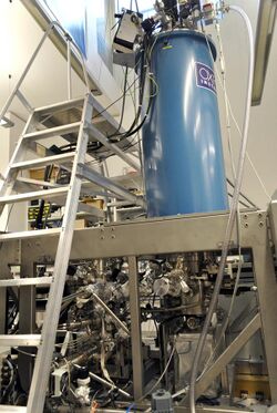
The main components of a scanning tunneling microscope are the scanning tip, piezoelectrically controlled height (z axis) and lateral (x and y axes) scanner, and coarse sample-to-tip approach mechanism. The microscope is controlled by dedicated electronics and a computer. The system is supported on a vibration isolation system.[5]
The tip is often made of tungsten or platinum–iridium wire, though gold is also used.[4] Tungsten tips are usually made by electrochemical etching, and platinum–iridium tips by mechanical shearing. The resolution of an image is limited by the radius of curvature of the scanning tip. Sometimes, image artefacts occur if the tip has more than one apex at the end; most frequently double-tip imaging is observed, a situation in which two apices contribute equally to the tunneling.[4] While several processes for obtaining sharp, usable tips are known, the ultimate test of quality of the tip is only possible when it is tunneling in the vacuum. Every so often the tips can be conditioned by applying high voltages when they are already in the tunneling range, or by making them pick up an atom or a molecule from the surface.
In most modern designs the scanner is a hollow tube of a radially polarized piezoelectric with metallized surfaces. The outer surface is divided into four long quadrants to serve as x and y motion electrodes with deflection voltages of two polarities applied on the opposing sides. The tube material is a lead zirconate titanate ceramic with a piezoelectric constant of about 5 nanometers per volt. The tip is mounted at the center of the tube. Because of some crosstalk between the electrodes and inherent nonlinearities, the motion is calibrated, and voltages needed for independent x, y and z motion applied according to calibration tables.[5]
Due to the extreme sensitivity of the tunneling current to the separation of the electrodes, proper vibration isolation or a rigid STM body is imperative for obtaining usable results. In the first STM by Binnig and Rohrer, magnetic levitation was used to keep the STM free from vibrations; now mechanical spring or gas spring systems are often employed.[5] Additionally, mechanisms for vibration damping using eddy currents are sometimes implemented. Microscopes designed for long scans in scanning tunneling spectroscopy need extreme stability and are built in anechoic chambers—dedicated concrete rooms with acoustic and electromagnetic isolation that are themselves floated on vibration isolation devices inside the laboratory.
Maintaining the tip position with respect to the sample, scanning the sample and acquiring the data is computer-controlled. Dedicated software for scanning probe microscopies is used for image processing as well as performing quantitative measurements.[10]
Some scanning tunneling microscopes are capable of recording images at high frame rates.[11][12] Videos made of such images can show surface diffusion[13] or track adsorption and reactions on the surface. In video-rate microscopes, frame rates of 80 Hz have been achieved with fully working feedback that adjusts the height of the tip.[14]
Principle of operation
Quantum tunneling of electrons is a functioning concept of STM that arises from quantum mechanics. Classically, a particle hitting an impenetrable barrier will not pass through. If the barrier is described by a potential acting along z direction, in which an electron of mass me acquires the potential energy U(z), the electron's trajectory will be deterministic and such that the sum E of its kinetic and potential energies is at all times conserved:
The electron will have a defined, non-zero momentum p only in regions where the initial energy E is greater than U(z). In quantum physics, however, particles with a very small mass, such as the electron, have discernible wavelike characteristics and are allowed to leak into classically forbidden regions. This is referred to as tunneling.[5]
Rectangular barrier model
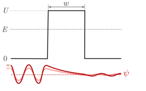
The simplest model of tunneling between the sample and the tip of a scanning tunneling microscope is that of a rectangular potential barrier.[15][5] An electron of energy E is incident upon an energy barrier of height U, in the region of space of width w. An electron's behavior in the presence of a potential U(z), assuming one-dimensional case, is described by wave functions that satisfy Schrödinger’s equation
where ħ is the reduced Planck’s constant, z is the position, and me is the electron mass. In the zero-potential regions on two sides of the barrier, the wave function takes on the forms
- for z < 0,
- for z > w,
where . Inside the barrier, where E < U, the wave function is a superposition of two terms, each decaying from one side of the barrier:
- for 0 < z < w,
where .
The coefficients r and t provide measure of how much of the incident electron's wave is reflected or transmitted through the barrier. Namely, of the whole impinging particle current only is transmitted, as can be seen from the probability current expression
which evaluates to . The transmission coefficient is obtained from the continuity condition on the three parts of the wave function and their derivatives at z = 0 and z = w (detailed derivation is in the article Rectangular potential barrier). This gives where . The expression can be further simplified, as follows:
In STM experiments, typical barrier height is of the order of the material's surface work function W, which for most metals has a value between 4 and 6 eV.[15] The work function is the minimum energy needed to bring an electron from an occupied level, the highest of which is the Fermi level (for metals at T = 0 K), to vacuum level. The electrons can tunnel between two metals only from occupied states on one side into the unoccupied states of the other side of the barrier. Without bias, Fermi energies are flush, and there is no tunneling. Bias shifts electron energies in one of the electrodes higher, and those electrons that have no match at the same energy on the other side will tunnel. In experiments, bias voltages of a fraction of 1 V are used, so is of the order of 10 to 12 nm−1, while w is a few tenths of a nanometer. The barrier is strongly attenuating. The expression for the transmission probability reduces to The tunneling current from a single level is therefore[15]
where both wave vectors depend on the level's energy E, and
Tunneling current is exponentially dependent on the separation of the sample and the tip, typically reducing by an order of magnitude when the separation is increased by 1 Å (0.1 nm).[5] Because of this, even when tunneling occurs from a non-ideally sharp tip, the dominant contribution to the current is from its most protruding atom or orbital.[15]
Tunneling between two conductors
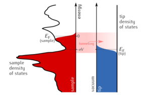
As a result of the restriction that the tunneling from an occupied energy level on one side of the barrier requires an empty level of the same energy on the other side of the barrier, tunneling occurs mainly with electrons near the Fermi level. The tunneling current can be related to the density of available or filled states in the sample. The current due to an applied voltage V (assume tunneling occurs from the sample to the tip) depends on two factors: 1) the number of electrons between the Fermi level EF and EF − eV in the sample, and 2) the number among them which have corresponding free states to tunnel into on the other side of the barrier at the tip.[5] The higher the density of available states in the tunneling region the greater the tunneling current. By convention, a positive V means that electrons in the tip tunnel into empty states in the sample; for a negative bias, electrons tunnel out of occupied states in the sample into the tip.[5]
For small biases and temperatures near absolute zero, the number of electrons in a given volume (the electron concentration) that are available for tunneling is the product of the density of the electronic states ρ(EF) and the energy interval between the two Fermi levels, eV.[5] Half of these electrons will be travelling away from the barrier. The other half will represent the electric current impinging on the barrier, which is given by the product of the electron concentration, charge, and velocity v (Ii = nev),[5]
The tunneling electric current will be a small fraction of the impinging current. The proportion is determined by the transmission probability T,[5] so
In the simplest model of a rectangular potential barrier the transmission probability coefficient T equals |t|2.
Bardeen's formalism

A model that is based on more realistic wave functions for the two electrodes was devised by John Bardeen in a study of the metal–insulator–metal junction.[16] His model takes two separate orthonormal sets of wave functions for the two electrodes and examines their time evolution as the systems are put close together.[5][15] Bardeen's novel method, ingenious in itself,[5] solves a time-dependent perturbative problem in which the perturbation emerges from the interaction of the two subsystems rather than an external potential of the standard Rayleigh–Schrödinger perturbation theory.
Each of the wave functions for the electrons of the sample (S) and the tip (T) decay into the vacuum after hitting the surface potential barrier, roughly of the size of the surface work function. The wave functions are the solutions of two separate Schrödinger's equations for electrons in potentials US and UT. When the time dependence of the states of known energies and is factored out, the wave functions have the following general form
If the two systems are put closer together, but are still separated by a thin vacuum region, the potential acting on an electron in the combined system is UT + US. Here, each of the potentials is spatially limited to its own side of the barrier. Only because the tail of a wave function of one electrode is in the range of the potential of the other, there is a finite probability for any state to evolve over time into the states of the other electrode.[5] The future of the sample's state μ can be written as a linear combination with time-dependent coefficients of and all :
with the initial condition .[5] When the new wave function is inserted into the Schrödinger’s equation for the potential UT + US, the obtained equation is projected onto each separate (that is, the equation is multiplied by a and integrated over the whole volume) to single out the coefficients All are taken to be nearly orthogonal to all (their overlap is a small fraction of the total wave functions), and only first-order quantities retained. Consequently, the time evolution of the coefficients is given by
Because the potential UT is zero at the distance of a few atomic diameters away from the surface of the electrode, the integration over z can be done from a point z0 somewhere inside the barrier and into the volume of the tip (z > z0).
If the tunneling matrix element is defined as
the probability of the sample's state μ evolving in time t into the state of the tip ν is
In a system with many electrons impinging on the barrier, this probability will give the proportion of those that successfully tunnel. If at a time t this fraction was at a later time t + dt the total fraction of would have tunneled. The current of tunneling electrons at each instance is therefore proportional to divided by which is the time derivative of [15]
The time scale of the measurement in STM is many orders of magnitude larger than the typical femtosecond time scale of electron processes in materials, and is large. The fraction part of the formula is a fast-oscillating function of that rapidly decays away from the central peak, where . In other words, the most probable tunneling process, by far, is the elastic one, in which the electron's energy is conserved. The fraction, as written above, is a representation of the delta function, so
Solid-state systems are commonly described in terms of continuous rather than discrete energy levels. The term can be thought of as the density of states of the tip at energy giving
The number of energy levels in the sample between the energies and is When occupied, these levels are spin-degenerate (except in a few special classes of materials) and contain charge of either spin. With the sample biased to voltage tunneling can occur only between states whose occupancies, given for each electrode by the Fermi–Dirac distribution , are not the same, that is, when either one or the other is occupied, but not both. That will be for all energies for which is not zero. For example, an electron will tunnel from energy level in the sample into energy level in the tip (), an electron at in the sample will find unoccupied states in the tip at (), and so will be for all energies in between. The tunneling current is therefore the sum of little contributions over all these energies of the product of three factors: representing available electrons, for those that are allowed to tunnel, and the probability factor for those that will actually tunnel:
Typical experiments are run at a liquid-helium temperature (around 4 K), at which the Fermi-level cut-off of the electron population is less than a millielectronvolt wide. The allowed energies are only those between the two step-like Fermi levels, and the integral becomes
When the bias is small, it is reasonable to assume that the electron wave functions and, consequently, the tunneling matrix element do not change significantly in the narrow range of energies. Then the tunneling current is simply the convolution of the densities of states of the sample surface and the tip:
How the tunneling current depends on distance between the two electrodes is contained in the tunneling matrix element
This formula can be transformed so that no explicit dependence on the potential remains. First, the part is taken out from the Schrödinger equation for the tip, and the elastic tunneling condition is used so that
Now is present in the Schrödinger equation for the sample and equals the kinetic plus the potential operator acting on However, the potential part containing US is on the tip side of the barrier nearly zero. What remains,
can be integrated over z because the integrand in the parentheses equals
Bardeen's tunneling matrix element is an integral of the wave functions and their gradients over a surface separating the two planar electrodes:
The exponential dependence of the tunneling current on the separation of the electrodes comes from the very wave functions that leak through the potential step at the surface and exhibit exponential decay into the classically forbidden region outside of the material.
The tunneling matrix elements show appreciable energy dependence, which is such that tunneling from the upper end of the eV interval is nearly an order of magnitude more likely than tunneling from the states at its bottom. When the sample is biased positively, its unoccupied levels are probed as if the density of states of the tip is concentrated at its Fermi level. Conversely, when the sample is biased negatively, its occupied electronic states are probed, but the spectrum of the electronic states of the tip dominates. In this case it is important that the density of states of the tip is as flat as possible.[5]
The results identical to Bardeen's can be obtained by considering adiabatic approach of the two electrodes and using the standard time-dependent perturbation theory.[15] This leads to Fermi's golden rule for the transition probability in the form given above.
Bardeen's model is for tunneling between two planar electrodes and does not explain scanning tunneling microscope's lateral resolution. Tersoff and Hamann[17][18][19] used Bardeen's theory and modeled the tip as a structureless geometric point.[5] This helped them disentangle the properties of the tip—which are hard to model—from the properties of the sample surface. The main result was that the tunneling current is proportional to the local density of states of the sample at the Fermi level taken at the position of the center of curvature of a spherically symmetric tip (s-wave tip model). With such a simplification, their model proved valuable for interpreting images of surface features bigger than a nanometer, even though it predicted atomic-scale corrugations of less than a picometer. These are well below the microscope's detection limit and below the values actually observed in experiments.
In sub-nanometer-resolution experiments, the convolution of the tip and sample surface states will always be important, to the extent of the apparent inversion of the atomic corrugations that may be observed within the same scan. Such effects can only be explained by modeling of the surface and tip electronic states and the ways the two electrodes interact from first principles.
Gallery of STM images
-
One-atom-thick silver islands grown on terraces of the (111) surface of palladium. Image size is 250 nm by 250 nm.
-
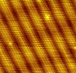
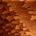
The characteristic reconstruction fringes on the (100) surface of gold are 1.44 nanometers wide[20] and consist of six atomic rows that sit on top of five rows of the crystal bulk. Image size is approximately 10 nm by 10 nm.
-
A 7 nm long part of a single-walled carbon nanotube.
-
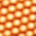
Atoms on the surface of a crystal of silicon carbide (SiC) are arranged in a hexagonal lattice and are 0.3 nm apart.
-
STM nanomanipulation of PTCDA molecules on graphite to inscribe the logo of the Center for NanoScience (CeNS), Munich.
Early invention
An earlier invention similar to Binnig and Rohrer's, the Topografiner of R. Young, J. Ward, and F. Scire from the NIST, relied on field emission.[21] However, Young is credited by the Nobel Committee as the person who realized that it should be possible to achieve better resolution by using the tunnel effect.[22]
Other related techniques
Many other microscopy techniques have been developed based upon STM. These include photon scanning microscopy (PSTM), which uses an optical tip to tunnel photons;[4] scanning tunneling potentiometry (STP), which measures electric potential across a surface;[4] spin-polarized scanning tunneling microscopy (SPSTM), which uses a ferromagnetic tip to tunnel spin-polarized electrons into a magnetic sample;[23] multi-tip scanning tunneling microscopy, which enables electrical measurements to be performed at the nanoscale; and atomic force microscopy (AFM), in which the force caused by interaction between the tip and sample is measured.
STM can be used to manipulate atoms and change the topography of the sample. This is attractive for several reasons. Firstly the STM has an atomically precise positioning system, which enables very accurate atomic-scale manipulation. Furthermore, after the surface is modified by the tip, the same instrument can be used to image the resulting structures. IBM researchers famously developed a way to manipulate xenon atoms adsorbed on a nickel surface.[4] This technique has been used to create electron corrals with a small number of adsorbed atoms and observe Friedel oscillations in the electron density on the surface of the substrate. Aside from modifying the actual sample surface, one can also use the STM to tunnel electrons into a layer of electron-beam photoresist on the sample, in order to do lithography. This has the advantage of offering more control of the exposure than traditional electron-beam lithography. Another practical application of STM is atomic deposition of metals (gold, silver, tungsten, etc.) with any desired (pre-programmed) pattern, which can be used as contacts to nanodevices or as nanodevices themselves.[citation needed]
See also
- Scanning probe microscopy
- Atomic force microscope
- Electrochemical scanning tunneling microscope
- Microscopy
- Electron microscope
- Multi-tip scanning tunneling microscopy
- IBM (atoms)
References
- ↑ "Scanning tunneling microscopy". IBM Journal of Research and Development 30 (4): 355–369. 1986. doi:10.1016/0039-6028(83)90716-1.
- ↑ "Scanning tunneling microscopy—from birth to adolescence". Reviews of Modern Physics 59 (3): 615–625. 1987-07-01. doi:10.1103/RevModPhys.59.615. Bibcode: 1987RvMP...59..615B.
- ↑ "Press release for the 1986 Nobel Prize in physics". http://nobelprize.org/nobel_prizes/physics/laureates/1986/press.html.
- ↑ 4.0 4.1 4.2 4.3 4.4 4.5 4.6 Scanning tunneling microscopy and its applications. New York: Springer Verlag. 2000. ISBN 978-3-540-65715-6. https://books.google.com/books?id=3Q08jRmmtrkC&pg=PA345.
- ↑ 5.00 5.01 5.02 5.03 5.04 5.05 5.06 5.07 5.08 5.09 5.10 5.11 5.12 5.13 5.14 5.15 5.16 5.17 5.18 5.19 5.20 Introduction to Scanning Tunneling Microscopy. Oxford University Press. 1993. ISBN 978-0-19-507150-4. http://www.columbia.edu/~jcc2161/documents/STM_book.pdf.
- ↑ SPECS. "STM 150 Aarhus – High Stability Temperature Control". http://www.specs.de/cms/upload/PDFs/ApplNotes/STM/ANote_HSTC-STM.pdf.
- ↑ Voigtländer, Bert (2015), Voigtländer, Bert, ed., "Scanning Tunneling Spectroscopy (STS)" (in en), Scanning Probe Microscopy: Atomic Force Microscopy and Scanning Tunneling Microscopy, NanoScience and Technology (Berlin, Heidelberg: Springer): pp. 309–334, doi:10.1007/978-3-662-45240-0_21, ISBN 978-3-662-45240-0, https://doi.org/10.1007/978-3-662-45240-0_21, retrieved 2020-10-15
- ↑ "STM References – Annotated Links for Scanning Tunneling Microscope Amateurs". http://www.e-basteln.de/index_r.htm.
- ↑ "Imaging the effects of individual zinc impurity atoms on superconductivity in Bi2Sr2CaCu2O8+delta". Nature 403 (6771): 746–750. February 2000. doi:10.1038/35001534. PMID 10693798. Bibcode: 2000Natur.403..746P.
- ↑ "Feature-oriented scanning probe microscopy" (PDF). Encyclopedia of Nanoscience and Nanotechnology. 14. USA: American Scientific Publishers. 2011. pp. 105–115. ISBN 978-1-58883-163-7. http://www.lapshin.fast-page.org/publications.htm#fospm2011.
- ↑ "Scanning probe microscopy at video-rate". Materials Today 11 (special issue): 40–48. 2008. doi:10.1016/S1369-7021(09)70006-9. ISSN 1369-7021.
- ↑ "Fast-acting piezoactuator and digital feedback loop for scanning tunneling microscopes" (PDF). Review of Scientific Instruments 64 (10): 2883–2887. 1993. doi:10.1063/1.1144377. Bibcode: 1993RScI...64.2883L. http://www.lapshin.fast-page.org/publications.htm#fast1993.
- ↑ "Direct measurement of surface diffusion using atom-tracking scanning tunneling microscopy". Physical Review Letters 76 (3): 459–462. January 1996. doi:10.1103/PhysRevLett.76.459. PMID 10061462. Bibcode: 1996PhRvL..76..459S. https://zenodo.org/record/1233907.
- ↑ "Scanning probe microscopes go video rate and beyond". Review of Scientific Instruments 76 (5): 053710–053710–9. 2005. doi:10.1063/1.1915288. ISSN 1369-7021. Bibcode: 2005RScI...76e3710R. https://openaccess.leidenuniv.nl/bitstream/handle/1887/61253/Review_of_Scientific_Instruments_78oe2005oe053710.pdf?sequence=1.
- ↑ 15.0 15.1 15.2 15.3 15.4 15.5 15.6 Lounis S (2014-04-03). "Theory of Scanning Tunneling Microscopy". arXiv:1404.0961 [cond-mat.mes-hall].
- ↑ "Tunneling from a many particle point of view". Phys. Rev. Lett. 6 (2): 57–59. 1961. doi:10.1103/PhysRevLett.6.57. Bibcode: 1961PhRvL...6...57B.
- ↑ "Theory and Application for the Scanning Tunneling Microscope". Physical Review Letters 50 (25): 1998–2001. 1983-06-20. doi:10.1103/PhysRevLett.50.1998. Bibcode: 1983PhRvL..50.1998T.
- ↑ "Theory of the scanning tunneling microscope". Physical Review B 31 (2): 805–813. January 1985. doi:10.1103/PhysRevB.31.805. PMID 9935822. Bibcode: 1985PhRvB..31..805T. https://link.aps.org/doi/10.1103/PhysRevB.31.805.
- ↑ Hansma, Paul K.; Tersoff, Jerry (1987-01-15). "Scanning tunneling microscopy". Journal of Applied Physics 61 (2): R1–R24. doi:10.1063/1.338189. ISSN 0021-8979. Bibcode: 1987JAP....61R...1H. https://aip.scitation.org/doi/10.1063/1.338189.
- ↑ "Electronic structure of reconstructed Au(100): Two-dimensional and one-dimensional surface states". Physical Review B 86 (4): 045426. 2012-07-18. doi:10.1103/PhysRevB.86.045426. Bibcode: 2012PhRvB..86d5426B.
- ↑ "The Topografiner: An Instrument for Measuring Surface Microtopography". Rev. Sci. Instrum. 43 (7): 999. 1972. doi:10.1063/1.1685846. Bibcode: 1972RScI...43..999Y. http://www.nanoworld.org/museum/young2.pdf.
- ↑ "The Topografiner: An Instrument for Measuring Surface Microtopography". NIST. http://nvl.nist.gov/pub/nistpubs/sp958-lide/214-218.pdf.
- ↑ "Recent advances in spin-polarized scanning tunneling microscopy". Ultramicroscopy 42–44: 338–344. 1992. doi:10.1016/0304-3991(92)90289-V.
Further reading
- Introduction to Scanning Tunneling Microscopy. Oxford University Press. 1993. ISBN 978-0-19-507150-4. http://www.columbia.edu/~jcc2161/documents/STM_book.pdf.
- Scanning probe microscopy and spectroscopy: methods and applications. Cambridge University Press. 1994. ISBN 978-0-521-42847-7. https://books.google.com/books?id=EXae0pjS2vwC.
- Scanning Tunneling Microscopy III – Theory of STM and Related Scanning Probe Methods. Springer Series in Surface Sciences. 29. Springer-Verlag Berlin Heidelberg. 1996. doi:10.1007/978-3-642-80118-1. ISBN 978-3-540-60824-0.
- Scanning tunneling microscopy and its applications. New York: Springer Verlag. 2000. ISBN 978-3-540-65715-6. https://books.google.com/books?id=3Q08jRmmtrkC&pg=PA345.
- (in en-gb) Scanning Probe Microscopy. NanoScience and Technology. 2015. doi:10.1007/978-3-662-45240-0. ISBN 978-3-662-45239-4. Bibcode: 2015spma.book.....V. https://link.springer.com/book/10.1007/978-3-662-45240-0.
- Lounis S (2014-04-03). "Theory of Scanning Tunneling Microscopy". arXiv:1404.0961 [cond-mat.mes-hall].
- "7 × 7 Reconstruction on Si(111) Resolved in Real Space" (in en). Physical Review Letters 50 (2): 120–123. 1983-01-10. doi:10.1103/PhysRevLett.50.120. ISSN 0031-9007. Bibcode: 1983PhRvL..50..120B.
- "Surface Studies by Scanning Tunneling Microscopy" (in en). Physical Review Letters 49 (1): 57–61. 1982-07-05. doi:10.1103/PhysRevLett.49.57. ISSN 0031-9007. Bibcode: 1982PhRvL..49...57B.
- "Tunneling through a controllable vacuum gap" (in en). Applied Physics Letters 40 (2): 178–180. 1982-01-15. doi:10.1063/1.92999. ISSN 0003-6951. Bibcode: 1982ApPhL..40..178B.
- "Tunnelling from a Many-Particle Point of View" (in en). Physical Review Letters 6 (2): 57–59. 1961-01-15. doi:10.1103/PhysRevLett.6.57. ISSN 0031-9007. Bibcode: 1961PhRvL...6...57B. https://link.aps.org/doi/10.1103/PhysRevLett.6.57.
- "Theory of the scanning tunneling microscope". Physical Review B 31 (2): 805–813. January 1985. doi:10.1103/PhysRevB.31.805. PMID 9935822. Bibcode: 1985PhRvB..31..805T. https://link.aps.org/doi/10.1103/PhysRevB.31.805.
- "Origin of atomic resolution on metal surfaces in scanning tunneling microscopy". Physical Review Letters 65 (4): 448–451. July 1990. doi:10.1103/PhysRevLett.65.448. PMID 10042923. Bibcode: 1990PhRvL..65..448C. https://link.aps.org/doi/10.1103/PhysRevLett.65.448.
- "Active nanocharacterization of nanofunctional materials by scanning tunneling microscopy". Science and Technology of Advanced Materials 9 (1): 013003. January 2008. doi:10.1088/1468-6996/9/1/013003. PMID 27877921. Bibcode: 2008STAdM...9a3003F.
External links
- A scanning tunelling microscope filmed during operation by an electron microscope
- The Inner Workings of an STM - An Animated Explanation WeCanFigureThisOut.org
- Build a simple STM with a cost of materials less than $100 excluding oscilloscope
- Animations and explanations on various types of microscopes including electron microscopes (Université Paris Sud)
- Introduction to STM in plain English (Harvard University)
 |
![The characteristic reconstruction fringes on the (100) surface of gold are 1.44 nanometers wide[20] and consist of six atomic rows that sit on top of five rows of the crystal bulk. Image size is approximately 10 nm by 10 nm.](/wiki/images/thumb/e/ec/Atomic_resolution_Au100.JPG/120px-Atomic_resolution_Au100.JPG)
