Physics:Ground bounce

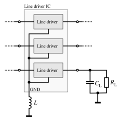
In electronic engineering, ground bounce is a phenomenon associated with transistor switching where the gate voltage can appear to be less than the local ground potential, causing the unstable operation of a logic gate.
Description
Ground bounce is usually seen on high density VLSI where insufficient precautions have been taken to supply a logic gate with a sufficiently low impedance connection to ground (or sufficiently high bypass capacitance). In this phenomenon, when the base of an NPN transistor is turned on, enough current flows through the emitter-collector circuit that the silicon in the immediate vicinity of the emitter-ground connection is pulled partially high, sometimes by several volts, thus raising the local ground, as perceived at the gate, to a value significantly above true ground. Relative to this local ground, the base voltage can go negative, thus shutting off the transistor. As the excess local charge dissipates, the transistor turns back on, possibly causing a repeat of the phenomenon, sometimes up to a half-dozen bounces.
Ground bounce is one of the leading causes of "hung" or metastable gates in modern digital circuit design. This happens because the ground bounce puts the input of a flip flop effectively at voltage level that is neither a one nor a zero at clock time, or causes untoward effects in the clock itself. A similar voltage sag phenomenon may be seen on the collector side, called supply voltage sag (or VCC sag), where VCC is pulled unnaturally low. As a whole, ground bounce is a major issue in nanometer range technologies in VLSI.
Ground bounce can also occur when the circuit board has poorly designed ground paths. Improper ground or VCC can lead to local variations in the ground level between various components. This is most commonly seen in circuit boards that have ground and VCC paths on the surfaces of the board.
Reduction
Ground bounce may be reduced by placing a 10–30-ohm resistor in series to each of the switching outputs to limit the current flow during the gate switch.[1]
See also
- Metastability in electronics
- Unbounded nondeterminism
- Buridan's ass
References
- Jeff Barrow, Reducing Ground Bounce, (2007), Analog Devices
- Vikas Kumar, Ground Bounce Primer, (2005), TechOnLine (now EETimes).
- Ground Bounce in 8-Bit High-Speed Logic, Pericom Application Note.
- AN-640 Understanding and Minimizing Ground Bounce, (2003) Fairchild Semiconductor, Application Note 640.
- Minimizing Ground Bounce & VCC Sag, White Paper, (2001) Altera Corporation.
- Ground Bounce part-1 and part-2 by Douglas Brooks,Articles, Ultra Cad Design.
 |
