Physics:Photoelectrowetting

Photoelectrowetting is a modification of the wetting properties of a surface (typically a hydrophobic surface) using incident light.[1]
Working principle
Whereas ordinary electrowetting is observed in surfaces consisting of a liquid/insulator/conductor stack, photoelectrowetting can be observed by replacing the conductor with a semiconductor to form a liquid/insulator/semiconductor stack. This has electrical and optical properties similar to the metal/insulator/semiconductor stack used in metal–oxide–semiconductor field effect transistors (MOSFETs) and charge-coupled devices (CCDs). Replacing the conductor with a semiconductor results in asymmetrical electrowetting behavior (in terms of voltage polarity), depending on the semiconductor doping type and density.
Incident light above the semiconductor's band gap creates photo-induced carriers via electron-hole pair generation in the depletion region of the underlying semiconductor. This leads to a modification of the capacitance of the insulator/semiconductor stack, resulting in a modification of the contact angle of a liquid droplet resting on the surface of the stack in a continuous way which can also be non-reversible.[2] The photoelectrowetting effect can be interpreted by a modification of the Young-Lippmann equation.[3]
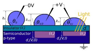
The figure illustrates the principle of the photoelectrowetting effect. At zero bias (0V) the conducting droplet has a large contact angle (left image) if the insulator is hydrophobic. As the bias is increased (positive for a p-type semiconductor, negative for an n-type semiconductor) the droplet spreads out – i.e. the contact angle decreases (middle image). In the presence of light (having an energy superior to the band gap of the semiconductor) the droplet spreads out more due to the reduction of the thickness of the space charge region at the insulator/semiconductor interface (right image).
Optical actuation of MEMS
Photoactuation of microelectromechanical systems (MEMS) has been demonstrated using photoelectrowetting.,[4][5] A microcantilever is placed on top of the liquid-insulator-photoconductor junction. As light is shined on the junction, the capillary force from the droplet on the cantilever, due to the contact angle change, deflects the cantilever. This wireless actuation can be used as a substitute for complex circuit-based systems currently used for optical addressing and control of autonomous wireless sensors[6]
Droplet transport
Photoelectrowetting can be used to circulate aqueous solution-based sessile droplets on a silicon wafer covered with silicon dioxide and Teflon – the latter providing a hydrophobic surface. Droplet transport is achieved by focusing a laser at the leading edge of the droplet. Droplet speeds of more than 10 mm/s can be achieved without the necessity of underlying patterned electrodes.[7]
See also
References
- ↑ S. Arscott, 'Moving liquids with light: Photoelectrowetting on semiconductors', Sci. Rep. 1, 184, (2011). Scientific Reports: Nature Publishing Group.
- ↑ Palma, Cesar; Deegan, Robert (5 January 2015). "Electrowetting on semiconductors". Applied Physics Letters 106 (1): 014106. doi:10.1063/1.4905348.
- ↑ Arscott, Steve (3 July 2014). "Electrowetting and semiconductors". RSC Advances 4 (55): 29223. doi:10.1039/c4ra04187a.
- ↑ Gaudet, Matthieu; Arscott, Steve (28 May 2012). "Optical actuation of microelectromechanical systems using photoelectrowetting". Applied Physics Letters 100 (22): 224103. doi:10.1063/1.4723569.
- ↑ "Research team creates photoelectrowetting circuit". http://phys.org/news/2012-01-team-photoelectrowetting-circuit.html.
- ↑ Yick, Jennifer, Biswanath Mukherjee, and Dipak Ghosal. "Wireless sensor network survey." Computer Networks 52.12 (2008): 2292-330. Web.
- ↑ C. Palma and R.D. Deegan "Droplet Translation Actuated by Photoelectrowetting" Langmuir 34, 3177 (2018). doi:10.1021/acs.langmuir.7b03340.
External links
- Institut d’Electronique, de Microélectronique et de Nanotechnologie (IEMN) - Centre National de la Recherche Scientifique (CNRS) - University of Lille
- The Deegan Group - University of Michigan
 |
