Physics:Quantum point contact

A quantum point contact (QPC) is a narrow constriction between two wide electrically conducting regions, of a width comparable to the electronic wavelength (nano- to micrometer).[1]
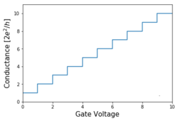
The importance of QPC lies in the fact that they prove quantisation of ballistic conductance in mesoscopic systems. The conductance of a QPC is quantized in units of , the so-called conductance quantum.
Quantum point contacts were first reported in 1988 by a Dutch team from Delft University of Technology and Philips Research[2] and, independently, by a British team from the Cavendish Laboratory.[3] They are based on earlier work by the British group which showed how split gates could be used to convert a two-dimensional electron gas into one-dimension, first in silicon[4] and then in gallium arsenide.[5][6]
This quantisation is reminiscent of the quantisation of the Hall conductance, but is measured in the absence of a magnetic field. The zero-field conductance quantisation and the smooth transition to the quantum Hall effect on applying a magnetic field are essentially consequences of the equipartition of current among an integer number of propagating modes in the constriction.
Fabrication
There are several different ways of fabricating a quantum point contact. It can be realized in a break-junction by pulling apart a piece of conductor until it breaks. The breaking point forms the point contact. In a more controlled way, quantum point contacts are formed in a two-dimensional electron gas (2DEG), e.g. in GaAs/AlGaAs heterostructures. By applying a voltage to suitably shaped gate electrodes, the electron gas can be locally depleted and many different types of conducting regions can be created in the plane of the 2DEG, among them quantum dots and quantum point contacts. Another means of creating a QPC is by positioning the tip of a scanning tunneling microscope close to the surface of a conductor.
Properties
Geometrically, a quantum point contact is a constriction in the transverse direction which presents a resistance to the motion of electrons. Applying a voltage
across the point contact induces a current to flow, the magnitude of this current is given by
, where
is the conductance of the contact. This formula resembles Ohm's law for macroscopic resistors. However, there is a fundamental difference here resulting from the small system size which requires a quantum mechanical analysis.[7]


It is most common to study QPC in two dimensional electron gases. This way the geometric constriction of the point contact turns the conductance through the opening to a one dimensional system. Moreover, it requires a quantum mechanical description of the system that results in the quantisation of conductance. Quantum mechanically, the current through the point contact is equipartitioned among the 1D subands, or transverse modes, in the constriction.
It is important to state that the previous discussion does not take into account possible transitions among modes. The Landauer formula can actually be generalized to express this possible transitions
,
where
is the transition matrix which incorporates non-zero probabilities of transmission from mode n to m.
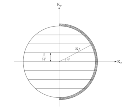
At low temperatures and voltages, unscattered and untrapped electrons contributing to the current have a certain energy/momentum/wavelength called Fermi energy/momentum/wavelength. Much like in a waveguide, the transverse confinement in the quantum point contact results in a "quantization" of the transverse motion—the transverse motion cannot vary continuously, but has to be one of a series of discrete modes. The waveguide analogy is applicable as long as coherence is not lost through scattering, e.g., by a defect or trapping site. The electron wave can only pass through the constriction if it interferes constructively, which for a given width of constriction, only happens for a certain number of modes . The current carried by such a quantum state is the product of the velocity times the electron density. These two quantities by themselves differ from one mode to the other, but their product is mode independent. As a consequence, each state contributes the same amount of per spin direction to the total conductance .
This is a fundamental result; the conductance does not take on arbitrary values but is quantized in multiples of the conductance quantum , which is expressed through the electron charge and the Planck constant . The integer number is determined by the width of the point contact and roughly equals the width divided by half the electron wavelength. As a function of the width of the point contact (or gate voltage in the case of GaAs/AlGaAs heterostructure devices), the conductance shows a staircase behavior as more and more modes (or channels) contribute to the electron transport. The step-height is given by .
On increasing the temperature, one finds experimentally that the plateaux acquire a finite slope until they are no longer resolved. This is a consequence of the thermal smearing of the Fermi-Dirac distribution. The conductance steps should disappear for (here ∆E is the subband splitting at the Fermi level). This is confirmed both by experiment and by numerical calculations.[9]
An external magnetic field applied to the quantum point contact lifts the spin degeneracy and leads to half-integer steps in the conductance. In addition, the number of modes that contribute becomes smaller. For large magnetic fields, is independent of the width of the constriction, given by the theory of the quantum Hall effect.
The 0.7 anomaly
Anomalous features on the quantized conductance steps are often observed in transport measurements of quantum point contacts. A notable example is the plateau at , the so-called 0.7-structure, arising due to enhanced electron-electron interactions arising from a smeared van Hove singularity in the local 1D density of states in the vicinity of the charge constriction.[10] Unlike the conductance steps, the 0.7-structure becomes more pronounced at higher temperature. 0.7-structure analogues are sometimes observed on higher conductance steps. Quasi-bound states arising from impurities, charge traps, and reflections within the constriction may also result in conductance structure close to the 1D limit.
Applications
Apart from studying fundamentals of charge transport in mesoscopic conductors, quantum point contacts can be used as extremely sensitive charge detectors. Since the conductance through the contact strongly depends on the size of the constriction, any potential fluctuation (for instance, created by other electrons) in the vicinity will influence the current through the QPC. It is possible to detect single electrons with such a scheme. In view of quantum computation in solid-state systems, QPCs can be used as readout devices for the state of a quantum bit (qubit).[11][12][13][14] In device physics, the configuration of QPCs is used for demonstrating a fully ballistic field-effect transistor.[15] Another application of the device is its use as a switch. A nickel wire is brought close enough to a gold surface and then, by the use of a piezoelectric actuator, the distance between the wire and the surface can be changed and thus, the transport characteristics of the device change between electron tunneling and ballistic.[16]
References
- ↑ H. van Houten; C.W.J. Beenakker (1996). "Quantum point contacts". Physics Today 49 (7): 22–27. doi:10.1063/1.881503. Bibcode: 1996PhT....49g..22V.
- ↑ B.J. van Wees (1988). "Quantized conductance of point contacts in a two-dimensional electron gas". Physical Review Letters 60 (9): 848–850. doi:10.1103/PhysRevLett.60.848. PMID 10038668. Bibcode: 1988PhRvL..60..848V.
- ↑ D.A. Wharam (1988). "One-dimensional transport and the quantization of the ballistic resistance". J. Phys. C 21 (8): L209–L214. doi:10.1088/0022-3719/21/8/002. Bibcode: 1988JPhC...21L.209W.
- ↑ C.C.Dean and M. Pepper (1982). "The transition from two- to one-dimensional electronic transport in narrow silicon accumulation layers". J. Phys. C 15 (36): L1287–L1297. doi:10.1088/0022-3719/15/36/005. Bibcode: 1982JPhC...15.1287D.
- ↑ T. J. Thornton (1986). "One-Dimensional Conduction in the 2D Electron Gas of a GaAs-AlGaAs Heterojunction". Physical Review Letters 56 (11): 1198–1201. doi:10.1103/PhysRevLett.56.1198. PMID 10032595. Bibcode: 1986PhRvL..56.1198T.
- ↑ K-F. Berggren (1986). "Magnetic Depopulation of 1D Subbands in a Narrow 2D Electron Gas in a GaAs:AlGaAs Heterojunction". Physical Review Letters 57 (14): 1769–1772. doi:10.1103/PhysRevLett.57.1769. PMID 10033540. Bibcode: 1986PhRvL..57.1769B.
- ↑ Pearsall, Thomas (2020). Quantum Photonics, 2nd edition. Graduate Texts in Physics. Springer. doi:10.1007/978-3-030-47325-9. ISBN 978-3-030-47324-2. https://www.springer.com/us/book/9783030473242.
- ↑ C.W.J.Beenakker and H. van Houten (1991). "Quantum Transport in Semiconductor Nanostructures". Solid State Physics 44: 1–228. doi:10.1016/s0081-1947(08)60091-0. ISBN 978-0-12-607744-5. Bibcode: 2004cond.mat.12664B.
- ↑ C.W.J.Beenakker and H. van Houten (1991). "Quantum Transport in Semiconductor Nanostructures". Solid State Physics 44: 1–228. doi:10.1016/s0081-1947(08)60091-0. ISBN 978-0-12-607744-5. Bibcode: 2004cond.mat.12664B.
- ↑ Bauer, Florian; Heyder, Jan; Schubert, Enrico; Borowsky, David; Taubert, Daniela; Bruognolo, Benedikt; Schuh, Dieter; Wegscheider, Werner et al. (September 2013). "Microscopic origin of the '0.7-anomaly' in quantum point contacts" (in en). Nature 501 (7465): 73–78. doi:10.1038/nature12421. ISSN 1476-4687. PMID 23995681. Bibcode: 2013Natur.501...73B. https://www.nature.com/articles/nature12421.
- ↑ J.M. Elzerman (2003). "Few-electron quantum dot circuit with integrated charge read out". Physical Review B 67 (16). doi:10.1103/PhysRevB.67.161308. Bibcode: 2003PhRvB..67p1308E.
- ↑ M. Field (1993). "Measurements of Coulomb blockade with a noninvasive voltage probe". Physical Review Letters 70 (9): 1311–1314. doi:10.1103/PhysRevLett.70.1311. PMID 10054344. Bibcode: 1993PhRvL..70.1311F.
- ↑ J. M. Elzerman (2004). "Single-shot read-out of an individual electron spin in a quantum dot". Nature 430 (6998): 431–435. doi:10.1038/nature02693. PMID 15269762. Bibcode: 2004Natur.430..431E.
- ↑ J. R. Petta (2005). "Coherent Manipulation of Coupled Electron Spins in Semiconductor Quantum Dots". Science 309 (5744): 2180–2184. doi:10.1126/science.1116955. PMID 16141370. Bibcode: 2005Sci...309.2180P.
- ↑ E. Gremion; D. Niepce; A. Cavanna; U. Gennser; Y. Jin (2010). "Evidence of a fully ballistic one-dimensional field-effect transistor: Experiment and simulation". Applied Physics Letters 97 (23): 233505. doi:10.1063/1.3521466. Bibcode: 2010ApPhL..97w3505G.
- ↑ Smith, D. P. E. (1995). "Quantum Point Contact Switches". Science 269 (5222): 371–3. doi:10.1126/science.269.5222.371. PMID 17841257. Bibcode: 1995Sci...269..371S. https://www.science.org/doi/10.1126/science.269.5222.371. Retrieved 30 May 2020.
Further reading
- C.W.J.Beenakker and H. van Houten (1991). "Quantum Transport in Semiconductor Nanostructures". Solid State Physics 44: 1–228. doi:10.1016/s0081-1947(08)60091-0. ISBN 978-0-12-607744-5. Bibcode: 2004cond.mat.12664B.
- K. J. Thomas (1996). "Possible spin polarization in a one-dimensional electron gas". Physical Review Letters 77 (1): 135–138. doi:10.1103/PhysRevLett.77.135. PMID 10061790. Bibcode: 1996PhRvL..77..135T.
- Nicolás Agraït; Alfredo Levy Yeyati; Jan M. van Ruitenbeek (2003). "Quantum properties of atomic-sized conductors". Physics Reports 377 (2–3): 81. doi:10.1016/S0370-1573(02)00633-6. Bibcode: 2003PhR...377...81A.
- Timp, G. (1992). "Chapter 3: When Does a Wire Become an Electron Waveguide". Semiconductors and Semimetals Volume 35. 35. pp. 113–190. doi:10.1016/S0080-8784(08)62393-5. ISBN 978-0-12-752135-0.
 |
