Physics:White light scanner

A white light scanner (WLS) is a device for performing surface height measurements of an object using coherence scanning interferometry (CSI) with spectrally-broadband, "white light" illumination. Different configurations of scanning interferometer may be used to measure macroscopic objects with surface profiles measuring in the centimeter range, to microscopic objects with surface profiles measuring in the micrometer range. For large-scale non-interferometric measurement systems, see structured-light 3D scanner.
Description
Vertical scanning interferometry is an example of low-coherence interferometry, which exploits the low coherence of white light. Interference will only be achieved when the path length delays of the interferometer are matched within the coherence time of the light source. VSI monitors the fringe contrast rather than the shape of the fringes.
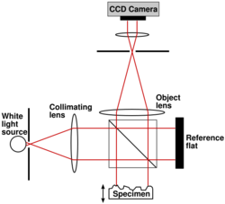
Fig. 2 illustrates a Twyman–Green interferometer set up for white light scanning of a macroscopic object. Light from the test specimen is mixed with light reflected from the reference mirror to form an interference pattern. Fringes appear in the CCD image only where the optical path lengths differ by less than half the coherence length of the light source, which is generally on the order of micrometers. The interference signal (correlogram) is recorded and analyzed as either the specimen or reference mirror is scanned. The focus position of any particular point on the surface of the specimen corresponds to the point of maximum fringe contrast (i.e. where the modulation of the correlogram is greatest).
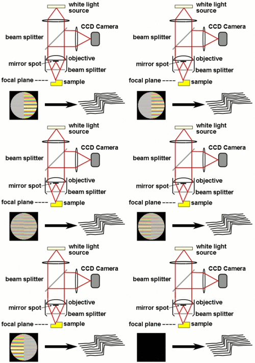
Fig. 3 illustrates a white light interferometric microscope using a Mirau interferometer in the objective. Other forms of interferometer used with white light include the Michelson interferometer (for low magnification objectives, where the reference mirror in a Mirau objective would interrupt too much of the aperture) and the Linnik interferometer (for high magnification objectives with limited working distance).[1] The objective (or alternatively, the sample) is moved vertically over the full height range of the sample, and the position of maximum fringe contrast is found for each pixel.[2][3]
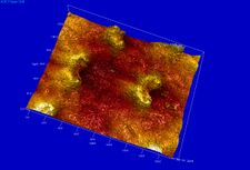
The chief benefit of low-coherence interferometry is that systems can be designed that do not suffer from the 2 pi ambiguity of coherent interferometry,[4][5][6] and as seen in Fig. 1, which scans a 180 μm × 140 μm × 10 μm volume, it is well suited to profiling steps and rough surfaces. The axial resolution of the system is determined by the coherence length of the light source and is typically in the micrometer range.[7][8][9] Industrial applications include in-process surface metrology, roughness measurement, 3D surface metrology in hard-to-reach spaces and in hostile environments, profilometry of surfaces with high aspect ratio features (grooves, channels, holes), and film thickness measurement (semi-conductor and optical industries, etc.).[10]
Technical
White-light interferometry scanning (WLS) systems capture intensity data at a series of positions along the vertical axis, determining where the surface is located by using the shape of the white-light interferogram, the localized phase of the interferogram, or a combination of both shape and phase. The white light interferogram actually consists of the superposition of fringes generated by multiple wavelengths, obtaining peak fringe contrast as a function of scan position, that is, the red portion of the object beam interferes with the red portion of the reference beam, the blue interferes with the blue, and so forth. In a WLS system, an imaging interferometer is vertically scanned to vary the optical path difference. During this process, a series of interference patterns are formed at each pixel in the instrument field of view. This results in an interference function, with interference varying as a function of optical path difference. The data are stored digitally and processed in a variety of ways depending on the system manufacturer, including being Fourier-transformed into frequency space, subject to cross-correlation methods, or analysis in the spatial domain.
If a Fourier transform is used, the original intensity data are expressed in terms of interference phase as a function of wavenumber. Wavenumber k is a representation of wavelength in the spatial frequency domain, defined by k = 2π/λ. If phase is plotted versus wavenumber, the slope of the function corresponds to the relative change in group-velocity optical path difference DG by Dh = DG/2nG where nG is group-velocity index of refraction. If this calculation is performed for each pixel, a three-dimensional surface height map emerges from the data.
In the actual measuring process, the optical path difference is steadily increased by scanning the objective vertically using a precision mechanical stage or piezoelectric positioner. Interference data are captured at each step in the scan. In effect, an interferogram is captured as a function of vertical position for each pixel in the detector array. To sift through the large amount of data acquired over long scans, many different techniques can be employed. Most methods allow the instrument to reject raw data that do not exhibit sufficient signal-to-noise. The intensity data as a function of the optical path difference are processed and converted to height information of the sample.
References
- ↑ Schmit, J.; Creath, K.; Wyant, J. C. (2007). "Surface Profilers, Multiple Wavelength, and White Light Intereferometry". Optical Shop Testing. pp. 667. doi:10.1002/9780470135976.ch15. ISBN 9780470135976.
- ↑ Harasaki, A.; Schmit, J.; Wyant, J. C. (2000). "Improved vertical-scanning interferometry". Applied Optics 39 (13): 2107–2115. doi:10.1364/AO.39.002107. PMID 18345114. Bibcode: 2000ApOpt..39.2107H. http://www.optics.arizona.edu/jcwyant/pdf/Published_Papers/Optical_Profiler/Improved%20Vertical-Scanning%20Interferometry.pdf. Retrieved 21 May 2012.
- ↑ "HDVSI - Introducing High Definition Vertical Scanning Interferometry for Nanotechnology Research from Veeco Instruments". Veeco. http://www.azom.com/article.aspx?ArticleID=4778.
- ↑ Plucinski, J.; Hypszer, R.; Wierzba, P.; Strakowski, M.; Jedrzejewska-Szczerska, M.; Maciejewski, M.; Kosmowski, B.B. (2008). "Optical low-coherence interferometry for selected technical applications". Bulletin of the Polish Academy of Sciences 56 (2): 155–172. http://bulletin.pan.pl/(56-2)155.pdf. Retrieved 8 April 2012.
- ↑ Yang, C.-H.; Wax, A; Dasari, R.R.; Feld, M.S. (2002). "2π ambiguity-free optical distance measurement with subnanometer precision with a novel phase-crossing low-coherence interferometer". Optics Letters 27 (2): 77–79. doi:10.1364/OL.27.000077. PMID 18007717. Bibcode: 2002OptL...27...77Y. http://authors.library.caltech.edu/3326/1/YANol02b.pdf.
- ↑ Hitzenberger, C. K.; Sticker, M.; Leitgeb, R.; Fercher, A. F. (2001). "Differential phase measurements in low-coherence interferometry without 2pi ambiguity". Optics Letters 26 (23): 1864–1866. doi:10.1364/ol.26.001864. PMID 18059719. Bibcode: 2001OptL...26.1864H.
- ↑ Wojtek J. Walecki, Kevin Lai, Vitalij Souchkov, Phuc Van, SH Lau, Ann Koo Physica Status Solidi C Volume 2, Issue 3 , Pages984 - 989
- ↑ W. J. Walecki et al. "Non-contact fast wafer metrology for ultra-thin patterned wafers mounted on grinding and dicing tapes" Electronics Manufacturing Technology Symposium, 2004. IEEE/CPMT/SEMI 29th International Volume , Issue , July 14–16, 2004 Page(s): 323 - 325
- ↑ "Services". http://www.zebraoptical.com/services.html.
- ↑ "Metrology Applications: Surface Roughness Measurement, Thickness, Volume Loss". http://www.novacam.com/applications/.
External links
- W. Bauer, "Special Properties of Coherence Scanning Interferometers for large Measurement Volumes" Journal of Physics: Conference Series Volume 311 Number 1, 012030: doi:10.1088/1742-6596/311/1/012030
- James C. Wyant
- W. J. Walecki, F. Szondy and M. M. Hilali "Fast in-line surface topography metrology enabling stress calculation for solar cell manufacturing for throughput in excess of 2000 wafers per hour" 2008 Meas. Sci. Technol. 19 025302 (6pp) doi:10.1088/0957-0233/19/2/025302
 |


