Engineering:AMD Phenom
 | |
| General Info | |
|---|---|
| Launched | November 19, 2007 |
| Marketed by | AMD |
| Designed by | AMD |
| Common manufacturer(s) | |
| Performance | |
| Max. CPU clock rate | 1.8 GHz to 2.6 GHz |
| HyperTransport speeds | 1.6 GHz to 2.0 GHz |
| Architecture and classification | |
| Min. feature size | 65 nm |
| Microarchitecture | K10 |
| Instruction set | MMX, SSE, SSE2, SSE3, SSE4a, x86-64, 3DNow! |
| Physical specifications | |
| Cores |
|
| Socket(s) | |
| History | |
| Predecessor | Athlon 64 X2 |
| Successor | Phenom II Athlon II |
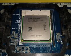
Phenom /fɪˈnɒm/ is the 64-bit AMD desktop processor line based on the K10 microarchitecture,[1] in what AMD calls family 10h (10 hex, i.e. 16 in normal decimal numbers) processors, sometimes incorrectly called "K10h". Triple-core versions (codenamed Toliman) belong to the Phenom 8000 series and quad cores (codenamed Agena) to the AMD Phenom X4 9000 series. The first processor in the family was released in 2007.
Background
AMD considers the quad core Phenoms to be the first "true" quad core design, as these processors are a monolithic multi-core design (all cores on the same silicon die), unlike Intel's Core 2 Quad series which are a multi-chip module (MCM) design. The processors are on the Socket AM2+ platform.[2]
Before Phenom's original release a flaw was discovered in the translation lookaside buffer (TLB) that could cause a system lock-up in rare circumstances; Phenom processors up to and including stepping "B2" and "BA" are affected by this bug. BIOS and software workarounds disable the TLB, and typically incur a performance penalty of at least 10%.[3] This penalty was not accounted for in pre-release previews of Phenom, hence the performance of early Phenoms delivered to customers may have been less than the preview benchmarks. "B3" stepping Phenom processors were released March 27, 2008 without the TLB bug and with "xx50" model numbers.[4]
An AMD subsidiary released a patch for the Linux kernel,[5] to overcome this bug by software emulation of accessed- and dirty-bits. This method causes less performance loss than previous workarounds. The program was said in December 2007 to have received "minimal functional testing."[6][7]
AMD launched several models of the Phenom processor in 2007 and 2008 and an upgraded Phenom II in late 2008.[8][9][10][11]
| AMD Phenom-based processor family | |||
|---|---|---|---|
| AMD K10 | Desktop | ||
| Quad-core | Triple-core | Dual-core | |

|

|
||
| Code-named | Agena | Toliman | Kuma |
| Core | 65 nm | 65 nm | 65 nm |
| Date released | Mar 2008 | Mar 2008 | Dec 2008 |
| List of AMD Phenom processors | |||
Features
CPU features table
Model naming methodology
The model numbers of the Phenom line of processors were changed from the PR system used in its predecessors, the AMD Athlon 64 processor family. The Phenom model numbering scheme, for-later released Athlon X2 processors, is a four-digit model number whose first digit is a family indicator.[12] Energy Efficient products end with an “e” suffix (for example, "Phenom 9350e"). Some Sempron processors use the prefix LE (for example, "Sempron LE-1200")
| Series number [13] | ||||
|---|---|---|---|---|
| Processor series | Family Indicator | |||
| Phenom X4 quad-core (Agena) | X4 9xxx | |||
| Phenom X3 triple-core (Toliman) | X3 8xxx | |||
| Athlon dual-core (Kuma) | X2 7xxx /6xxx | |||
| Athlon single-core (Lima) | 1 | |||
| Sempron single-core (Sparta) | 1 | |||
Cores
Phenom X4
Agena (65 nm SOI)

- Four AMD K10 cores
- L1 cache: 64 KB + 64 KB[14] (data + instructions) per core
- L2 cache: 512 KB per core, full-speed
- L3 cache: 2 MB shared among all cores
- Memory controller: dual channel DDR2-1066 MHz with unganging option
- MMX, Extended 3DNow!, SSE, SSE2, SSE3, SSE4a, AMD64, Cool'n'Quiet, NX bit, AMD-V
- Socket AM2+, HyperTransport with 1600 to 2000 MHz
- Power consumption (TDP): 65, 95, 125 and 140 Watt
- First release
- November 19, 2007 (B2 Stepping)
- March 27, 2008 (B3 Stepping)
- Clock rate: 1800 to 2600 MHz
- Models: Phenom X4 9100e to 9950
Phenom X3
Toliman (65 nm SOI)

- Three AMD K10 cores chip harvested from Agena with one core disabled[15]
- L1 cache: 64 KB data and 64 KB instruction cache per core
- L2 cache: 512 KB per core, full-speed
- L3 cache: 2 MB shared between all cores
- Memory controller: dual channel DDR2-1066 MHz with unganging option
- MMX, Extended 3DNow!, SSE, SSE2, SSE3, SSE4a, AMD64, Cool'n'Quiet, NX bit, AMD-V
- Socket AM2+, HyperTransport with 1600 to 1800 MHz
- Power consumption (TDP): 65 and 95 Watt
- First release
- March 27, 2008 (B2 Stepping)
- April 23, 2008 (B3 Stepping)
- Clock rate: 2100 to 2500 MHz
- Models: Phenom X3 8250e to 8850
See also
References
- ↑ "AMD to Drop "Athlon" Moniker on the High End". DailyTech. May 2, 2007. http://dailytech.com/AMD+to+Drop+Athlon+Moniker+on+the+High+End/article7136.htm.
- ↑ "More Details on AMD "Stars" Chipsets". DailyTech. May 3, 2007. http://dailytech.com/More+Details+on+AMD+Stars+Chipsets/article7147.htm.
- ↑ "Phenom TLB patch benchmarked: A look at how AMD's BIOS workaround impacts Phenom performance". techreport.com. December 6, 2007. http://techreport.com/articles.x/13741/4.
- ↑ "High Performance AMD Phenom X4 Processors Lead the Charge to HD Desktop Gaming and Video". AMD. March 27, 2008. https://www.amd.com/us-en/Corporate/VirtualPressRoom/0,,51_104_543_15434~124395,00.html.
- ↑ "AMD Family 10h revision B2 Erratum 298 and L2 Eviction Bug Workaround". AMD. December 5, 2007. http://www.x86-64.org/pipermail/discuss/2007-December/010260.html.
- ↑ Cyril Kowaliski (2007-12-05). "Linux kernel patch reveals TLB bug's workings". The Tech Report. http://techreport.com/discussions.x/13742.
- ↑ Scott Wasson (2007-12-06). "Phenom TLB patch benchmarked". The Tech Report. http://techreport.com/articles.x/13741.
- ↑ "Final AMD "Stars" Models Unveiled". DailyTech. May 4, 2007. http://www.dailytech.com/Final+AMD+Stars+Models+Unveiled+/article7157.htm.
- ↑ "AMD Expands Upcoming Processor Branding". DailyTech. June 4, 2007. http://www.dailytech.com/amd+expands+upcoming+processor+branding/article7537.htm.
- ↑ "How to decipher AMD's new CPU naming code". Gadget Lab. 2007-06-04. http://blog.wired.com/gadgets/2007/06/how_to_decipher.html.
- ↑ "Model Number and Feature Comparisons AMD Athlon 64 X2 Dual-Core and AMD Athlon X2 Dual-Core Processors". 2007. https://www.amd.com/us-en/Processors/ProductInformation/0,,30_118_9485_13041%5E13076,00.html.
- ↑ "AMD Revised Desktop Model Number Structure". VR-Zone. October 9, 2007. http://www.vr-zone.com/articles/AMD_Revised_Desktop_Model_Number_Structure/5330.html.
- ↑ VR-Zone report . Retrieved October 9, 2007.
- ↑ In this article, the conventional prefixes for computer memory denote base-2 values whereby “kilobyte” (KB) = 210 bytes.
- ↑ "List of Unlockable AMD CPUs". https://docs.google.com/spreadsheets/d/19Ms49ip5PBB7nYnf5urxsySvH-Sdy6liE2EBDaB8b54.
External links
