Nanometrology

Nanometrology is a subfield of metrology, concerned with the science of measurement at the nanoscale level. Nanometrology has a crucial role in order to produce nanomaterials and devices with a high degree of accuracy and reliability in nanomanufacturing.
A challenge in this field is to develop or create new measurement techniques and standards to meet the needs of next-generation advanced manufacturing, which will rely on nanometer scale materials and technologies. The needs for measurement and characterization of new sample structures and characteristics far exceed the capabilities of current measurement science. Anticipated advances in emerging U.S. nanotechnology industries will require revolutionary metrology with higher resolution and accuracy than has previously been envisioned.[1]
Introduction
Control of the critical dimensions are the most important factors in nanotechnology. Nanometrology today, is to a large extent based on the development in semiconductor technology. Nanometrology is the science of measurement at the nanoscale level. Nanometer or nm is equivalent to 10^-9 m. In Nanotechnology accurate control of dimensions of objects is important. Typical dimensions of nanosystems vary from 10 nm to a few hundred nm and while fabricating such systems measurement up to 0.1 nm is required.
At nanoscale due to the small dimensions various new physical phenomena can be observed. For example, when the crystal size is smaller than the electron mean free path the conductivity of the crystal changes. Another example is the discretization of stresses in the system. It becomes important to measure the physical parameters so as to apply these phenomena into engineering of nanosystems and manufacturing them. The measurement of length or size, force, mass, electrical and other properties is included in Nanometrology. The problem is how to measure these with reliability and accuracy. The measurement techniques used for macro systems cannot be directly used for measurement of parameters in nanosystems. Various techniques based on physical phenomena have been developed which can be used for measure or determine the parameters for nanostructures and nanomaterials. Some of the popular ones are X-Ray diffraction, transmission electron microscopy, High Resolution Transmission Electron Microscopy, atomic force microscopy, scanning electron microscopy, field emission scanning electron microscopy and Brunauer, Emmett, Teller method to determine specific surface.
Nanotechnology is an important field because of the large number of applications it has and it has become necessary to develop more precise techniques of measurement and globally accepted standards. Hence progress is required in the field of Nanometrology.
Development needs
Nanotechnology can be divided into two branches. The first being molecular nanotechnology which involves bottom up manufacturing and the second is engineering nanotechnology which involve the development and processing of materials and systems at nanoscale. The measurement and manufacturing tools and techniques required for the two branches are slightly different.
Furthermore, Nanometrology requirements are different for the industry and research institutions. Nanometrology of research has progressed faster than that for industry mainly because implementing nanometrology for industry is difficult. In research oriented nanometrology resolution is important whereas in industrial nanometrology accuracy is given precedence over resolution. Further, due to economic reasons it is important to have low time costs in industrial nanometrology, whereas it is not important for research nanometrology. The various measurement techniques available today require a controlled environment like in vacuum, vibration and noise free environment. Also, in industrial nanometrology requires that the measurements be more quantitative with minimum number of parameters.
Standards
International standards
Metrology standards are objects or ideas that are designated as being authoritative for some accepted reason. Whatever value they possess is useful for comparison to unknowns for the purpose of establishing or confirming an assigned value based on the standard. The execution of measurement comparisons for the purpose of establishing the relationship between a standard and some other measuring device is calibration. The ideal standard is independently reproducible without uncertainty. The worldwide market for products with nanotechnology applications is projected to be at least a couple of hundred billion dollars in the near future.[citation needed] Until recently, there almost no established internationally accepted standards for nanotechnology related field. The International Organization for Standardization TC-229 Technical Committee on Nanotechnology recently published few standards for terminology, characterization of nanomaterials and nanoparticles using measurement tools like AFM, SEM, Interferometers, optoacoustic tools, gas adsorption methods etc. Certain standards for standardization of measurements for electrical properties have been published by the International Electrotechnical Commission. Some important standards which are yet to be established are standards for measuring thickness of thin films or layers, characterization of surface features, standards for force measurement at nanoscale, standards for characterization of critical dimensions of nanoparticles and nanostructures and also Standards for measurement for physical properties like conductivity, elasticity etc.
National standards
Because of the importance of nanotechnology in the future, countries around the world have programmes to establish national standards for nanometrology and nanotechnology. These programmes are run by the national standard agencies of the respective countries. In the United States, National Institute of Standards and Technology has been working on developing new techniques for measurement at nanoscale and has also established some national standards for nanotechnology. These standards are for nanoparticle characterization, Roughness Characterization, magnification standard, calibration standards etc.
Calibration
It is difficult to provide samples using which precision instruments can be calibrated at nanoscale. Reference or calibration standards are important for repeatability to be ensured. But there are no international standards for calibration and the calibration artefacts provided by the company along with their equipment is only good for calibrating that particular equipment. Hence it is difficult to select a universal calibration artefact using which we can achieve repeatability at nanoscale. At nanoscale while calibrating care needs to be taken for influence of external factors like vibration, noise, motions caused by thermal drift and creep, nonlinear behaviour and hysteresis of piezoscanner[2] and internal factors like the interaction between the artefact and the equipment which can cause significant deviations.
Measurement techniques
In the last 70 years various techniques for measuring at nanoscale have been developed. Most of them based on some physical phenomena observed on particle interactions or forces at nanoscale. Some of the most commonly used techniques are Atomic Force Microscopy, X-Ray Diffraction, Scanning Electron Microscopy, Transmission Electron Microscopy, High Resolution Transmission Electron Microscopy, and Field Emission Scanning Electron Microscopy.
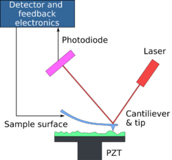
Atomic force microscopy (AFM) is one of the most common measurement techniques. It can be used to measure topology, grain size, frictional characteristics and different forces. It consists of a silicon cantilever with a sharp tip with a radius of curvature of a few nanometers. The tip is used as a probe on the specimen to be measured. The forces acting at the atomic level between the tip and the surface of the specimen cause the tip to deflect and this deflection is detected using a laser spot which is reflected to an array of photodiodes.
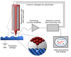
Scanning tunneling microscopy (STM) is another instrument commonly used. It is used to measure 3-D topology of the specimen. The STM is based on the concept of quantum tunneling. When a conducting tip is brought very near to the surface to be examined, a bias (voltage difference) applied between the two can allow electrons to tunnel through the vacuum between them. Measurements are made by monitoring the current as the tip's position scans across the surface, which can then be used to display an image.
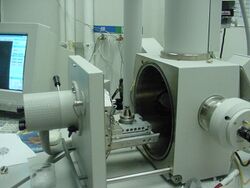
Another commonly used instrument is the scanning electron microscopy (SEM) which apart from measuring the shape and size of the particles and topography of the surface can be used to determine the composition of elements and compounds the sample is composed of. In SEM the specimen surface is scanned with a high energy electron beam. The electrons in the beam interact with atoms in the specimen and interactions are detected using detectors. The interactions produced are back scattering of electrons, transmission of electrons, secondary electrons etc. To remove high angle electrons magnetics lenses are used.
The instruments mentioned above produce realistic pictures of the surface are excellent measuring tools for research. Industrial applications of nanotechnology require the measurements to be produced need to be more quantitative. The requirement in industrial nanometrology is for higher accuracy than resolution as compared to research nanometrology.
Nano coordinate measuring machine
A coordinate measuring machine (CMM) that works at the nanoscale would have a smaller frame than the CMM used for macroscale objects. This is so because it may provide the necessary stiffness and stability to achieve nanoscale uncertainties in x,y and z directions. The probes for such a machine need to be small to enable a 3-D measurement of nanometre features from the sides and from inside like nanoholes. Also for accuracy laser interferometers need to be used. NIST has developed a surface measuring instrument, called the Molecular Measuring Machine. This instrument is basically an STM. The x- and y-axes are read out by laser interferometers. The molecules on the surface area can be identified individually and at the same time the distance between any two molecules can be determined. For measuring with molecular resolution, the measuring times become very large for even a very small surface area. Ilmenau Machine is another nanomeasuring machine developed by researchers at the Ilmenau University of Technology.
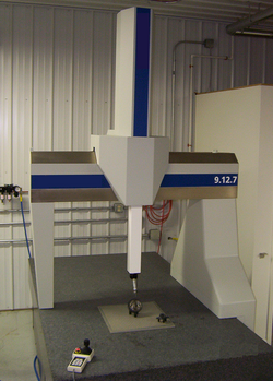
The components of a nano CMM include nanoprobes, control hardware, 3D-nanopositioning platform, and instruments with high resolution and accuracy for linear and angular measurement.
List of some of the measurement techniques
Traceability
In metrology at macro scale achieving traceability is quite easy and artefacts like scales, laser interferometers, step gauges, and straight edges are used. At nanoscale a crystalline highly oriented pyrolytic graphite (HOPG), mica or silicon surface is considered suitable used as calibration artefact for achieving traceability.[4][5] But it is not always possible to ensure traceability. Like what is a straight edge at nanoscale and even if take the same standard as that for macroscale there is no way to calibrate it accurately at nanoscale. This so because the requisite internationally or nationally accepted reference standards are not always there. Also the measurement equipment required to ensure traceability has not been developed. The generally used for traceability are miniaturisation of traditional metrology standards hence there is a need for establishing nanoscale standards. Also there is a need to establish some kind of uncertainty estimation model. Traceability is one of the fundamental requirements for manufacturing and assembly of products when multiple producers are there.
Tolerance
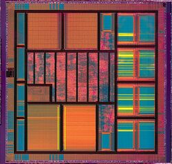
Tolerance is the permissible limit or limits of variation in dimensions, properties, or conditions without significantly affecting functioning of equipment or a process. Tolerances are specified to allow reasonable leeway for imperfections and inherent variability without compromising performance. In nanotechnology the systems have dimensions in the range of nanometers. Defining tolerances at nanoscale with suitable calibration standards for traceability is difficult for different nanomanufacturing methods. There are various integration techniques developed in the semiconductor industry that are used in nanomanufacturing.
Integration techniques
- In hetero integration direct fabrication of nanosystems from compound substrates is done. Geometric tolerances are required to achieve the functionality of the assembly.
- In hybrid integration nanocomponents are placed or assembled on a substrate fabricating functioning nanosystems. In this technique, the most important control parameter is the positional accuracy of the components on the substrate.
- In monolithic integration all the fabrication process steps are integrated on a single substrate and hence no mating of components or assembly is required. The advantage of this technique is that the geometric measurements are no longer of primary importance for achieving functionality of nanosystem or control of the fabrication process.
Classification of nanostructures
There are a variety of nanostructures like nanocomposites, nanowires, nanopowders, nanotubes, fullerenes nanofibers, nanocages, nanocrystallites, nanoneedles, nanofoams, nanomeshes, nanoparticles, nanopillars, thin films, nanorods, nanofabrics, quantumdots etc. The most common way to classify nano structures is by their dimensions.

Dimensional classification
| Dimensions | Criteria | Examples |
|---|---|---|
| Zero-dimensional (0-D) | The nanostructure has all dimensions in the nanometer range. | Nanoparticles, quantum dots, nanodots |
| One-dimensional (1-D) | One dimension of the nanostructure is outside the nanometer range. | Nanowires, nanorods, nanotubes |
| Two-dimensional (2-D) | Two dimensions of the nanostructure are outside the nanometer range. | Coatings, thin-film-multilayers |
| Three-dimensional (3-D) | Three dimensions of the nanostructure are outside the nanometer range. | Bulk |
Classification of grain structure
Nanostructures can be classified on the basis of the grain structure and size there are made up of. This is applicable in the cas of 2-dimensional and 3-Dimensional Nanostructurs.
Surface area measurement
For nanopowder to determine the specific surface area the B.E.T. method is commonly used. The drop of pressure of nitrogen in a closed container due to adsorption of the nitrogen molecules to the surface of the material inserted in the container is measured. Also, the shape of the nanopowder particles is assumed to be spherical.
- D = 6/(ρ*A)
Where "D" is the effective diameter, "ρ" is the density and "A" is the surface area found from the B.E.T. method.
See also
References
- ↑ 1.0 1.1 "Programs of the Manufacturing Engineering Laboratory". March 2008. http://www.mel.nist.gov/programs/pbookweb.pdf. Template:PD-inline
- ↑ R. V. Lapshin (2004). "Feature-oriented scanning methodology for probe microscopy and nanotechnology". Nanotechnology (UK: IOP) 15 (9): 1135–1151. doi:10.1088/0957-4484/15/9/006. ISSN 0957-4484. Bibcode: 2004Nanot..15.1135L. http://www.lapshin.fast-page.org/publications/R.%20V.%20Lapshin,%20Feature-oriented%20scanning%20methodology%20for%20probe%20microscopy%20and%20nanotechnology.pdf. (Russian translation is available).
- ↑ "Co-Nanomet: Nanometrology in Europe". http://www.co-nanomet.eu:80/.
- ↑ R. V. Lapshin (1998). "Automatic lateral calibration of tunneling microscope scanners". Review of Scientific Instruments (USA: AIP) 69 (9): 3268–3276. doi:10.1063/1.1149091. ISSN 0034-6748. Bibcode: 1998RScI...69.3268L. http://www.lapshin.fast-page.org/publications/R.%20V.%20Lapshin,%20Automatic%20lateral%20calibration%20of%20tunneling%20microscope%20scanners.pdf.
- ↑ R. V. Lapshin (2019). "Drift-insensitive distributed calibration of probe microscope scanner in nanometer range: Real mode". Applied Surface Science (Netherlands: Elsevier B. V.) 470: 1122–1129. doi:10.1016/j.apsusc.2018.10.149. ISSN 0169-4332. Bibcode: 2019ApSS..470.1122L.
General references
- Whitehouse, David J. (2011). Handbook of surface and nanometrology. CRC Press. ISBN 9781420082012. OCLC 703152969.
- Schulte, Jürgen (2005). Nanotechnology: global strategies, industry trends and applications. Wiley. ISBN 9780470854006. OCLC 56733161.
- "Eighth Nanoforum Report: Nanometrology". July 2006. http://nanoparticles.org/pdf/nanometrology.pdf.
- Aliofkhazraei, Mahmood; Rouhaghdam, Alireza Sabour (2010). "Synthesis and Processing of Nanostructured Films, and Introduction to and Comparison with Plasma Electrolysis". Fabrication of nanostructures by plasma electrolysis. Wiley-VCH. ISBN 9783527326754. OCLC 676709104. https://application.wiley-vch.de/books/sample/3527326758_c01.pdf.
 |
