Focused ion beam
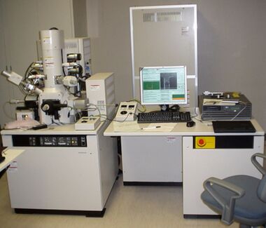
Focused ion beam, also known as FIB, is a technique used particularly in the semiconductor industry, materials science and increasingly in the biological field for site-specific analysis, deposition, and ablation of materials. A FIB setup is a scientific instrument that resembles a scanning electron microscope (SEM). However, while the SEM uses a focused beam of electrons to image the sample in the chamber, a FIB setup uses a focused beam of ions instead. FIB can also be incorporated in a system with both electron and ion beam columns, allowing the same feature to be investigated using either of the beams. FIB should not be confused with using a beam of focused ions for direct write lithography (such as in proton beam writing). These are generally quite different systems where the material is modified by other mechanisms.
Ion beam source
Most widespread instruments are using liquid metal ion sources (LMIS), especially gallium ion sources. Ion sources based on elemental gold and iridium are also available. In a gallium LMIS, gallium metal is placed in contact with a tungsten needle, and heated gallium wets the tungsten and flows to the tip of the needle, where the opposing forces of surface tension and electric field form the gallium into a cusp shaped tip called a Taylor cone. The tip radius of this cone is extremely small (~2 nm). The huge electric field at this small tip (greater than 1×10⁸ volts per centimeter) causes ionization and field emission of the gallium atoms.
Source ions are then generally accelerated to an energy of 1–50 kiloelectronvolts (0.16–8.01 fJ), and focused onto the sample by electrostatic lenses. LMIS produce high current density ion beams with very small energy spread. A modern FIB can deliver tens of nanoamperes of current to a sample, or can image the sample with a spot size on the order of a few nanometers.
More recently, instruments using plasma beams of noble gas ions, such as xenon, have become available more widely.[1]
Principle
Focused ion beam (FIB) systems have been produced commercially for approximately twenty years, primarily for large semiconductor manufacturers. FIB systems operate in a similar fashion to a scanning electron microscope (SEM) except, rather than a beam of electrons and as the name implies, FIB systems use a finely focused beam of ions (usually gallium) that can be operated at low beam currents for imaging or at high beam currents for site specific sputtering or milling.
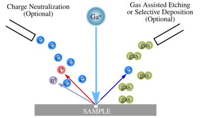
As the diagram on the right shows, the gallium (Ga+) primary ion beam hits the sample surface and sputters a small amount of material, which leaves the surface as either secondary ions (i+ or i−) or neutral atoms (n0). The primary beam also produces secondary electrons (e−). As the primary beam rasters on the sample surface, the signal from the sputtered ions or secondary electrons is collected to form an image.
At low primary beam currents, very little material is sputtered and modern FIB systems can easily achieve 5 nm imaging resolution (imaging resolution with Ga ions is limited to ~5 nm by sputtering[2][3] and detector efficiency). At higher primary currents, a great deal of material can be removed by sputtering, allowing precision milling of the specimen down to a sub micrometer or even a nano scale.
If the sample is non-conductive, a low energy electron flood gun can be used to provide charge neutralization. In this manner, by imaging with positive secondary ions using the positive primary ion beam, even highly insulating samples may be imaged and milled without a conducting surface coating, as would be required in an SEM.
Until recently, the overwhelming usage of FIB has been in the semiconductor industry. Such applications as defect analysis, circuit modification, photomask repair and transmission electron microscope (TEM) sample preparation of site specific locations on integrated circuits have become commonplace procedures. The latest FIB systems have high resolution imaging capability; this capability coupled with in situ sectioning has eliminated the need, in many cases, to examine FIB sectioned specimens in a separate SEM instrument.[4] SEM imaging is still required for the highest resolution imaging and to prevent damage to sensitive samples. However, the combination of SEM and FIB columns onto the same chamber enables the benefits of both to be utilized.
FIB imaging
At lower beam currents, FIB imaging resolution begins to rival the more familiar scanning electron microscope (SEM) in terms of imaging topography, however the FIB's two imaging modes, using secondary electrons and secondary ions, both produced by the primary ion beam, offer many advantages over SEM.
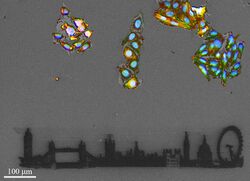
FIB secondary electron images show intense grain orientation contrast. As a result, grain morphology can be readily imaged without resorting to chemical etching. Grain boundary contrast can also be enhanced through careful selection of imaging parameters. FIB secondary ion images also reveal chemical differences, and are especially useful in corrosion studies, as secondary ion yields of metals can increase by three orders of magnitude in the presence of oxygen, clearly revealing the presence of corrosion.[7]
Another advantage of FIB secondary electron imaging is the fact that the ion beam does not alter the signal from fluorescent probes used in the labelling of proteins, thus creating the opportunity to correlate FIB secondary electron images with images obtained by fluorescence microscopes.[5][6]
Etching
Unlike an electron microscope, FIB is inherently destructive to the specimen. When the high-energy gallium ions strike the sample, they will sputter atoms from the surface. Gallium atoms will also be implanted into the top few nanometers of the surface, and the surface will be made amorphous.
Because of the sputtering capability, the FIB is used as a micro- and nano-machining tool, to modify or machine materials at the micro- and nanoscale. FIB micro machining has become a broad field of its own, but nano machining with FIB is a field that is still developing. Commonly the smallest beam size for imaging is 2.5–6 nm. The smallest milled features are somewhat larger (10–15 nm) as this is dependent on the total beam size and interactions with the sample being milled.
FIB tools are designed to etch or machine surfaces, an ideal FIB might machine away one atom layer without any disruption of the atoms in the next layer, or any residual disruptions above the surface. Yet currently because of the sputter the machining typically roughens surfaces at the sub-micrometer length scales.[8][9]
Deposition
A FIB can also be used to deposit material via ion beam induced deposition. FIB-assisted chemical vapor deposition occurs when a gas, such as tungsten hexacarbonyl (W(CO)6) is introduced to the vacuum chamber and allowed to chemisorb onto the sample. By scanning an area with the beam, the precursor gas will be decomposed into volatile and non-volatile components; the non-volatile component, such as tungsten, remains on the surface as a deposition. This is useful, as the deposited metal can be used as a sacrificial layer, to protect the underlying sample from the destructive sputtering of the beam. From nanometers to hundred of micrometers in length, tungsten metal deposition allows metal lines to be put right where needed. Other materials such as platinum, cobalt, carbon, gold, etc., can also be locally deposited.[8][9] Gas assisted deposition and FIB etching process are shown below.[10]
FIB is often used in the semiconductor industry to patch or modify an existing semiconductor device. For example, in an integrated circuit, the gallium beam could be used to cut unwanted electrical connections, and/or to deposit conductive material in order to make a connection. The high level of surface interaction is exploited in patterned doping of semiconductors. FIB is also used for maskless implantation.
For TEM preparation
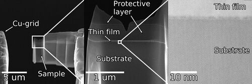
The FIB is also commonly used to prepare samples for the transmission electron microscope. The TEM requires very thin samples, typically ~100 nanometers or less. Other techniques, such as ion milling or electropolishing can be used to prepare such thin samples. However, the nanometer-scale resolution of the FIB allows the exact region of interest to be chosen, such as perhaps a grain boundary or defect in a material. This is vital, for example, in integrated circuit failure analysis. If a particular transistor out of several million on a chip is bad, the only tool capable of preparing an electron microscope sample of that single transistor is the FIB.[8][9] The same protocol used for preparing samples to transmission electron microscopy can also be used to select a micro area of a sample, extract it and prepare it for analysis using a Secondary ion mass spectrometry (SIMS).[11]
The drawbacks to FIB sample preparation are the above-mentioned surface damage and implantation, which produce noticeable effects when using techniques such as high-resolution "lattice imaging" TEM or electron energy loss spectroscopy. This damaged layer can be minimized by FIB milling with lower beam voltages, or by further milling with a low-voltage argon ion beam after completion of the FIB process.[12]
FIB preparation can be used with cryogenically frozen samples in a suitably equipped instrument, allowing cross sectional analysis of samples containing liquids or fats, such as biological samples, pharmaceuticals, foams, inks, and food products.[13]
FIB is also used for secondary ion mass spectrometry (SIMS). The ejected secondary ions are collected and analyzed after the surface of the specimen has been sputtered with a primary focused ion beam.
For transfer of sensitive samples
For a minimal introduction of stress and bending to transmission electron microscopy (TEM) samples (lamellae, thin films, and other mechanically and beam sensitive samples), when transferring inside a focused ion beam (FIB), flexible metallic nanowires can be attached to a typically rigid micromanipulator.
The main advantages of this method include a significant reduction of sample preparation time (quick welding and cutting of nanowire at low beam current), and minimization of stress-induced bending, Pt contamination, and ion beam damage.[14]
This technique is particularly suitable for in situ electron microscopy sample preparation.
For Atom Probe sample preparation
The same successive milling steps applied when making TEM samples can be applied to make conical samples for atom probe tomography. In this case the ion moved in an annular milling pattern with the inner milling circle being made progressively smaller. The beam current is generally reduced the smaller the inner circle becomes to avoid damaging or destroying the sample.[15]
FIB tomography
The focused ion beam has become a powerful tool for site-specific 3D imaging of sub-micron features in a sample. In this FIB tomography technique, the sample is sequentially milled using an ion beam perpendicular to the specimen while imaging the newly exposed surface using an electron beam. This so-called, slice and view approach allows larger scale nano-structures to be characterized across the many imaging modes available to an SEM, including secondary electron, backscattered electron, and energy dispersive x-ray measurement. The process is destructive, since the specimen is being sequentially milled away after each image is collected. The collected series of images is then reconstructed to a 3D volume by registering the image stack and removing artifacts. The predominant artifact that degrades FIB tomography is ion mill curtaining, where mill patterns form large aperiodic stripes in each image. The ion mill curtaining can be removed using destriping algorithms. FIB tomography can be done at both room and cryo temperatures as well as on both materials and biological samples.
History
History of FIB technology
- 1975: The first FIB systems based on field emission technology were developed by Levi-Setti[16][17] and by Orloff and Swanson[18] and used gas field ionization sources (GFISs).
- 1978: The first FIB based on an LMIS was built by Seliger et al.[19]
Physics of LMIS
- 1600: Gilbert documented that fluid under high tension forms a cone.
- 1914: Zeleny observed and filmed cones and jets
- 1959: Feynman suggested the use of ion beams.
- 1964: Taylor produced exactly conical solution to equations of electro hydrodynamics (EHD)
- 1975: Krohn and Ringo produced first high brightness ion source: LMIS
Some pioneers of LMIS and FIB[20]
- Mahoney (1969)
- Sudraud et al. Paris XI Orsay (1974)
- Hughes Research Labs, Seliger (1978)
- Hughes Research Labs, Kubena (1978–1993)
- University of Oxford Mair (1980)
- Culham UK, Roy Clampitt Prewett (1980)
- Oregon Graduate Center, L. Swanson (1980)
- Oregon Graduate Center, J. Orloff (1974)
- MIT, J. Melngailis (1980)
Helium ion microscope (HeIM)
Another ion source seen in commercially available instruments is a helium ion source, which is inherently less damaging to the sample than Ga ions although it will still sputter small amounts of material especially at high magnifications and long scan times. As helium ions can be focused into a small probe size and provide a much smaller sample interaction than high energy (>1 kV) electrons in the SEM, the He ion microscope can generate equal or higher resolution images with good material contrast and a higher depth of focus. Commercial instruments are capable of sub 1 nm resolution.[21][22]
Wien filter in focused ion beam setup
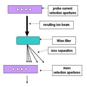
Imaging and milling with Ga ions always result in Ga incorporation near the sample surface. As the sample surface is sputtered away at a rate proportional to the sputtering yield and the ion flux (ions per area per time), the Ga is implanted further into the sample, and a steady-state profile of Ga is reached. This implantation is often a problem in the range of the semiconductor where silicon can be amorphised by the gallium. In order to get an alternative solution to Ga LMI sources, mass-filtered columns have been developed, based on a Wien filter technology. Such sources include Au-Si, Au-Ge and Au-Si-Ge sources providing Si, Cr, Fe, Co, Ni, Ge, In, Sn, Au, Pb and other elements.
The principle of a Wien filter is based on the equilibrium of the opposite forces induced by perpendicular electrostatic and a magnetic fields acting on accelerated particles. The proper mass trajectory remains straight and passes through the mass selection aperture while the other masses are stopped.[23]
Besides allowing the use of sources others than gallium, these columns can switch from different species simply by adjusting the properties of the Wien filter. Larger ions can be used to make rapid milling before refining the contours with smaller ones. Users also benefits from the possibility to dope their samples with elements of suitable alloy sources.
The latter property has found great interests in the investigation of magnetic materials and devices. Khizroev and Litvinov have shown, with the help of magnetic force microscopy (MFM), that there is a critical dose of ions that a magnetic material can be exposed to without experiencing a change in the magnetic properties. Exploiting FIB from such an unconventional perspective is especially favourable today when the future of so many novel technologies depends on the ability to rapidly fabricate prototype nanoscale magnetic devices.[24]
See also
- Confocal microscopy
- Ion milling machine
- Powder diffraction
- Ultrafast x-ray
- X-ray crystallography
- X-ray scattering techniques
References
- ↑ Burnett, T.L.; Kelley, R.; Winiarski, B.; Contreras, L.; Daly, M.; Gholinia, A.; Burke, M.G.; Withers, P.J. (2016-02-01). "Large volume serial section tomography by Xe Plasma FIB dual beam microscopy" (in en). Ultramicroscopy 161: 119–129. doi:10.1016/j.ultramic.2015.11.001. ISSN 0304-3991. PMID 26683814.
- ↑ Orloff, Jon (1996). "Fundamental limits to imaging resolution for focused ion beams". Journal of Vacuum Science and Technology B 14 (6): 3759–3763. doi:10.1116/1.588663. Bibcode: 1996JVSTB..14.3759O.
- ↑ Castaldo, V.; Hagen, C. W.; Rieger, B.; Kruit, P. (2008). "Sputtering limits versus signal-to-noise limits in the observation of Sn balls in a Ga[sup + microscope"]. Journal of Vacuum Science and Technology B 26 (6): 2107–2115. doi:10.1116/1.3013306. Bibcode: 2008JVSTB..26.2107C. http://repository.tudelft.nl/islandora/object/uuid%3A283ec59c-b0ec-4932-aef4-7ef63808ce7c/datastream/OBJ/view.
- ↑ "Introduction : Focused Ion Beam Systems". http://www.fibics.com/fib/tutorials/introduction-focused-ion-beam-systems/4/.
- ↑ 5.0 5.1 Smith, C (2012). "Microscopy: Two microscopes are better than one". Nature 492 (7428): 293–297. doi:10.1038/492293a. PMID 23235883. Bibcode: 2012Natur.492..293S.
- ↑ 6.0 6.1 Bertazzo, S. (2012). "Correlative Light-Ion Microscopy for Biological Applications". Nanoscale 4 (9): 2851–2854. doi:10.1039/c2nr30431g. PMID 22466253. Bibcode: 2012Nanos...4.2851B.
- ↑ "FIB: Chemical Contrast". http://www.fibics.com/MS_FIBApp_SII_SteelCorrosion.html.
- ↑ 8.0 8.1 8.2 J. Orloff; M. Utlaut; L. Swanson (2003). High Resolution Focused Ion Beams: FIB and Its Applications. Springer Press. ISBN 978-0-306-47350-0. https://books.google.com/books?id=DGlJG-lcBLsC.
- ↑ 9.0 9.1 9.2 L.A. Giannuzzi; F.A. Stevens (2004). Introduction to Focused Ion Beams: Instrumentation, Theory, Techniques and Practice. Springer Press. ISBN 978-0-387-23116-7.
- ↑ Koch, J.; Grun, K.; Ruff, M.; Wernhardt, R.; Wieck, A.D. (1999). "Creation of nanoelectronic devices by focused ion beam implantation". 1. pp. 35–39. doi:10.1109/IECON.1999.822165. ISBN 0-7803-5735-3.
- ↑ Bertazzo, Sergio; Maidment, Susannah C. R.; Kallepitis, Charalambos; Fearn, Sarah; Stevens, Molly M.; Xie, Hai-nan (9 June 2015). "Fibres and cellular structures preserved in 75-million–year-old dinosaur specimens". Nature Communications 6: 7352. doi:10.1038/ncomms8352. PMID 26056764. Bibcode: 2015NatCo...6.7352B.
- ↑ Principe, E L; Gnauck, P; Hoffrogge, P (2005). "A Three Beam Approach to TEM Preparation Using In-situ Low Voltage Argon Ion Final Milling in a FIB-SEM Instrument". Microscopy and Microanalysis 11. doi:10.1017/S1431927605502460.
- ↑ "Unique Imaging of Soft Materials Using Cryo-SDB". http://www.fei.com/uploadedFiles/Documents/Content/2006_06_CryoSDB_SoftImaging_AppNote_mb.pdf.
- ↑ Gorji, Saleh; Kashiwar, Ankush; Mantha, Lakshmi S; Kruk, Robert; Witte, Ralf; Marek, Peter; Hahn, Horst; Kübel, Christian et al. (December 2020). "Nanowire facilitated transfer of sensitive TEM samples in a FIB". Ultramicroscopy 219: 113075. doi:10.1016/j.ultramic.2020.113075. PMID 33035837. https://www.researchgate.net/publication/342952945.
- ↑ Miller, M. K.; Russell, K. F. (September 2007). "Atom probe specimen preparation with a dual beam SEM/FIB miller". Ultramicroscopy 107 (9): 761–6. doi:10.1016/j.ultramic.2007.02.023. PMID 17403581. https://www.sciencedirect.com/science/article/abs/pii/S030439910700054X.
- ↑ Levi-Setti, R. (1974). "Proton scanning microscopy: feasibility and promise". Scanning Electron Microscopy: 125.
- ↑ W. H. Escovitz; T. R. Fox; R. Levi-Setti (1975). "Scanning Transmission Ion Microscope with a Field Ion Source". Proceedings of the National Academy of Sciences of the United States of America 72 (5): 1826–1828. doi:10.1073/pnas.72.5.1826. PMID 1057173. Bibcode: 1975PNAS...72.1826E.
- ↑ Orloff, J.; Swanson, L. (1975). "Study of a field-ionization source for microprobe applications". Journal of Vacuum Science and Technology 12 (6): 1209. doi:10.1116/1.568497. Bibcode: 1975JVST...12.1209O.
- ↑ Seliger, R.; Ward, J.W.; Wang, V.; Kubena, R.L. (1979). "A high-intensity scanning ion probe with submicrometer spot size". Appl. Phys. Lett. 34 (5): 310. doi:10.1063/1.90786. Bibcode: 1979ApPhL..34..310S.
- ↑ C.A. Volkert; A.M. Minor (2007). "Focused Ion Beam: Microscopy and Micromachining". MRS Bulletin 32 (5): 389–399. doi:10.1557/mrs2007.62. http://www.nanolab.ucla.edu/pdf/mrs_bulletin_2007_fib_machining.pdf.
- ↑ "Carl Zeiss press release". 2008-11-21. http://www.smt.zeiss.com/C1256A770030BCE0/WebViewAllE/F4BF4E46C9379912C1257508002B9F7C.
- ↑ "Zeiss Orion Helium Ion Microscope Technical Data". http://www.smt.zeiss.com/C1256E4600307C70/EmbedTitelIntern/ORIONEssentialSpecificationPDF/$File/oriondata.pdf.
- ↑ Orsay physics work on ExB mass filter Column, 1993
- ↑ Khizroev S.; Litvinov D. (2004). "Focused-ion-beam-based rapid prototyping of nanoscale magnetic devices". Nanotechnology 15 (3): R7. doi:10.1088/0957-4484/15/3/R01. Bibcode: 2004Nanot..15R...7K.
- Hoffman, David P.; Shtengel, Gleb; Xu, C. Shan; Campbell, Kirby R.; Freeman, Melanie; Wang, Lei; Milkie, Daniel E.; Pasolli, H. Amalia et al. (2020). "Correlative three-dimensional super-resolution and block-face electron microscopy of whole vitreously frozen cells". Science 367 (6475): eaaz5357. doi:10.1126/science.aaz5357. ISSN 0036-8075. PMID 31949053.
Further reading
- Mackenzie, R A D (1990). "Focused ion beam technology: a bibliography". Nanotechnology 1 (2): 163–201. doi:10.1088/0957-4484/1/2/007. Bibcode: 1990Nanot...1..163M.
- J. Orloff (2009). Handbook of Charged Particle Optics. CRC Press. ISBN 978-1-4200-4554-3. https://books.google.com/books?id=y0FF19lud5YC.
- L.A. Giannuzzi; F.A. Stevie (2004). Introduction to Focused Ion Beams: Instrumentation, Theory, Techniques and Practice. Springer Press. ISBN 978-0-387-23116-7.
 |
