Physics:Optical properties of carbon nanotubes
| Part of a series of articles on |
| Nanomaterials |
|---|
 |
| Carbon nanotubes |
| Fullerenes |
| Other nanoparticles |
| Nanostructured materials |
|
|
The optical properties of carbon nanotubes are highly relevant for materials science. The way carbon nanotubes interact with electromagnetic radiation is unique in many respects, as evidenced by their peculiar absorption, photoluminescence (fluorescence), and Raman spectra.
Carbon nanotubes are unique "one-dimensional" materials, whose hollow fibers (tubes) have a unique and highly ordered atomic and electronic structure, and can be made in a wide range of dimension. The diameter typically varies from 0.4 to 40 nm (i.e., a range of ~100 times). However, the length can reach 55.5 cm (21.9 in), implying a length-to-diameter ratio as high as 132,000,000:1; which is unequaled by any other material.[1] Consequently, all the electronic, optical, electrochemical and mechanical properties of the carbon nanotubes are extremely anisotropic (directionally dependent) and tunable.[2]
Applications of carbon nanotubes in optics and photonics are still less developed than in other fields. Some properties that may lead to practical use include tuneability and wavelength selectivity. Potential applications that have been demonstrated include light emitting diodes (LEDs),[3] bolometers[4] and optoelectronic memory.[5]
Apart from direct applications, the optical properties of carbon nanotubes can be very useful in their manufacture and application to other fields. Spectroscopic methods offer the possibility of quick and non-destructive characterization of relatively large amounts of carbon nanotubes, yielding detailed measurements of non-tubular carbon content, tube type and chirality, structural defects, and many other properties that are relevant to those other applications.
Geometric structure
Chiral angle
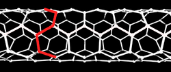
A single-walled carbon nanotube (SWNT[6] or SWCNT[7]) can be envisioned as strip of a graphene molecule (a single sheet of graphite) rolled and joined into a cylinder. The structure of the nanotube can be characterized by the width of the diameter d of the tube and the angle (θ) of the strip relative to the main symmetry axes of the hexagonal graphene lattice. This angle, which varies from 0 to 30 degrees, is called the "chiral angle" of the tube[7] and varies dependent on the conditions of nanotube growth.[6]
(n, m) notation

The nanotube structure can be described by two integer indices (n,m) that describe the width and direction of that hypothetical strip as coordinates in a fundamental reference frame of the graphene lattice. If the atoms around any 6-member ring of the graphene are numbered sequentially from 1 to 6, the two vectors u and v of that frame are the displacements from atom 1 to atoms 3 and 5, respectively. Those two vectors have the same length, and their directions are 60 degrees apart. The vector w = n u + m v is then interpreted as the circumference of the unrolled tube on the graphene lattice; it relates each point A1 on one edge of the strip to the point A2 on the other edge that will be identified with it as the strip is rolled up. The chiral angle α is then the angle between u and w.[8][9][10]
The pairs (n, m) that describe distinct tube structures are those with 0 ≤ m ≤ n and n > 0. All geometric properties of the tube, such as diameter, chiral angle, and symmetries, can be computed from these indices.[7][11]
The type also determines the electronic structure of the tube. Specifically, the tube behaves like a metal if m − n is a multiple of 3, and like a semiconductor otherwise.[12] Thus, across the available indices, one third of SWNTs are metallic, and two thirds are semiconducting.[13] Truly metallic carbon nanotubes with minimal to nonexistent band gap have been defined only as those where n = m.[11]
Zigzag and armchair tubes
Tubes of type (n, m) with n = m (chiral angle = 30°) are called "armchair" and those with m = 0 (chiral angle = 0°) "zigzag".[14] All other chiral angles produce what are known as chiral nanotubes.[15]
 |
 |
Electronic structure
The optical properties of carbon nanotubes are largely determined by their unique electronic structure. The rolling up of the graphene lattice affects that structure in ways that depend strongly on the geometric structure type (n, m).[13]
Van Hove singularities
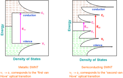

A characteristic feature of one-dimensional crystals is that their distribution of density of states (DOS) is not a continuous function of energy, but it descends gradually and then increases in a discontinuous spike. These sharp peaks are called Van Hove singularities.[16] In contrast, three-dimensional (bulk) materials have continuous DOS.[17][18]
Van Hove singularities result in the following optical properties of carbon nanotubes:
- Optical transitions occur between the v1 − c1, v2 − c2, etc., states of semiconducting or metallic nanotubes and are traditionally labeled as S11, S22, M11, etc., or, if the "conductivity" of the tube is unknown or unimportant, as E11, E22, etc.[18] Crossover transitions c1 − v2, c2 − v1, etc., are dipole-forbidden and thus are extremely weak, but they were possibly observed using cross-polarized optical geometry.[19]
- The energies between the Van Hove singularities depend on the nanotube structure. Thus by varying this structure, one can tune the optoelectronic properties of carbon nanotube. Such fine tuning has been experimentally demonstrated using UV illumination of polymer-dispersed CNTs.[20]
- Optical transitions are rather sharp (~10 meV) and strong. Consequently, it is relatively easy to selectively excite nanotubes having certain (n, m) indices, as well as to detect optical signals from individual nanotubes.[18]
Kataura plot
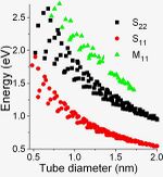
The band structure of carbon nanotubes having certain (n, m) indexes can be calculated.[21] A theoretical graph based on these calculations was designed in 1999 by Hiromichi Kataura to rationalize experimental findings. A Kataura plot relates the nanotube diameter and its bandgap energies for all nanotubes in a diameter range.[22] The oscillating shape of every branch of the Kataura plot reflects the intrinsic strong dependence of the SWNT properties on the (n, m) index rather than on its diameter.[23]
Optical properties
Optical absorption

Optical absorption in carbon nanotubes differs from absorption in conventional 3D materials by presence of sharp peaks (1D nanotubes) instead of an absorption threshold followed by an absorption increase (most 3D solids). Absorption in nanotubes originates from electronic transitions from the v2 to c2 (energy E22) or v1 to c1 (E11) levels, etc.[8][22] The transitions are relatively sharp and can be used to identify nanotube types. Note that the sharpness deteriorates with increasing energy, and that many nanotubes have very similar E22 or E11 energies, and thus significant overlap occurs in absorption spectra. This overlap is avoided in photoluminescence mapping measurements (see below), which instead of a combination of overlapped transitions identifies individual (E22, E11) pairs.[24][25]
Optical absorption is routinely used to quantify quality of the carbon nanotube powders.[26]
The spectrum is analyzed in terms of intensities of nanotube-related peaks, background and pi-carbon peak; the latter two mostly originate from non-nanotube carbon in contaminated samples. However, it has been recently shown that by aggregating nearly single chirality semiconducting nanotubes into closely packed Van der Waals bundles the absorption background can be attributed to free carrier transition originating from intertube charge transfer.[27]
Carbon nanotubes as a black body
These SWNT forests (buckypaper) were grown by the super-growth CVD method to about 10 μm height. Two factors could contribute to strong light absorption by these structures: (i) a distribution of CNT chiralities resulted in various bandgaps for individual CNTs. Thus a compound material was formed with broadband absorption. (ii) Light might be trapped in those forests due to multiple reflections.[28][29][30]
| UV-to-near IR | Near-to-mid IR | Mid-to-far IR | |
|---|---|---|---|
| Wavelength, μm | 0.2–2 | 2–20 | 25–200 |
| Incident angle, ° | 8 | 5 | 10 |
| Reflection | Hemispherical-directional | Hemispherical-directional | Specular |
| Reference | White reflectance standard | Gold mirror | Aluminum mirror |
| Average reflectance | 0.0160 | 0.0097 | 0.0017 |
| Standard deviation | 0.0048 | 0.0041 | 0.0027 |
Luminescence

Photoluminescence (fluorescence)
Semiconducting single-walled carbon nanotubes emit near-infrared light upon photoexcitation, described interchangeably as fluorescence or photoluminescence (PL).[32] The excitation of PL usually occurs as follows: an electron in a nanotube absorbs excitation light via S22 transition, creating an electron-hole pair (exciton). Both electron and hole rapidly relax (via phonon-assisted processes) from c2 to c1 and from v2 to v1 states, respectively. Then they recombine through a c1 − v1 transition resulting in light emission.[16]
No excitonic luminescence can be produced in metallic tubes.[16] Their electrons can be excited, thus resulting in optical absorption,[33] but the holes are immediately filled by other electrons out of the many available in the metal. Therefore, no excitons are produced.
Salient properties
- Photoluminescence from SWNT, as well as optical absorption and Raman scattering, is linearly polarized along the tube axis.[34] This allows monitoring of the SWNTs orientation without direct microscopic observation. * PL is quick: relaxation typically occurs within 100 picoseconds.[35]
- PL efficiency was first found to be low (~0.01%),[35] but later studies measured much higher quantum yields. By improving the structural quality and isolation of nanotubes, emission efficiency increased. A quantum yield of 1% was reported in nanotubes sorted by diameter and length through gradient centrifugation,[36] and it was further increased to 20% by optimizing the procedure of isolating individual nanotubes in solution.[37]
- The spectral range of PL is rather wide. Emission wavelength can vary between 0.8 and 2.1 micrometers depending on the nanotube structure.[24][25]
- Excitons are apparently delocalized over several nanotubes in single chirality bundles as the photoluminescence spectrum displays a splitting consistent with intertube exciton tunneling.[27]
- Interaction between nanotubes or between a nanotube and another material may quench or increase PL.[38] No PL is observed in multi-walled carbon nanotubes. PL from double-wall carbon nanotubes strongly depends on the preparation method: CVD grown DWCNTs show emission both from inner and outer shells.[24][25] However, DWCNTs produced by encapsulating fullerenes into SWNTs and annealing show PL only from the outer shells.[39] Isolated SWNTs lying on the substrate show extremely weak PL which has been detected in few studies only.[40] Detachment of the tubes from the substrate drastically increases PL.
- Position of the (S22, S11) PL peaks depends slightly (within 2%) on the nanotube environment (air, dispersant, etc.). However, the shift depends on the (n, m) index, and thus the whole PL map not only shifts, but also warps upon changing the CNT medium.
Raman scattering
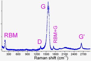
Raman spectroscopy has good spatial resolution (~0.5 micrometers) and sensitivity (single nanotubes); it requires only minimal sample preparation and is rather informative. Consequently, Raman spectroscopy is probably the most popular technique of carbon nanotube characterization. Raman scattering in SWNTs is resonant, i.e., only those tubes are probed which have one of the bandgaps equal to the exciting laser energy.[41][42] Several scattering modes dominate the SWNT spectrum, as discussed below.
Similar to photoluminescence mapping, the energy of the excitation light can be scanned in Raman measurements, thus producing Raman maps.[41] Those maps also contain oval-shaped features uniquely identifying (n, m) indices. Contrary to PL, Raman mapping detects not only semiconducting but also metallic tubes, and it is less sensitive to nanotube bundling than PL. However, requirement of a tunable laser and a dedicated spectrometer is a strong technical impediment.
Radial breathing mode
Radial breathing mode (RBM) corresponds to radial expansion-contraction of the nanotube. Therefore, its frequency νRBM (in cm−1) depends on the nanotube diameter d as, νRBM = A/d + B (where A and B are constants dependent on the environment in which the nanotube is present. For example, B=0 for individual nanotubes.) (in nanometers) and can be estimated[41][42] as νRBM = 234/d + 10 for SWNT or νRBM = 248/d for DWNT, which is very useful in deducing the CNT diameter from the RBM position. Typical RBM range is 100–350 cm−1. If RBM intensity is particularly strong, its weak second overtone can be observed at double frequency.
Bundling mode
The bundling mode is a special form of RBM supposedly originating from collective vibration in a bundle of SWNTs.[43]
G mode
D mode
G′ mode
Anti-Stokes scattering
All the above Raman modes can be observed both as Stokes and anti-Stokes scattering. As mentioned above, Raman scattering from CNTs is resonant in nature, i.e. only tubes whose band gap energy is similar to the laser energy are excited. The difference between those two energies, and thus the band gap of individual tubes, can be estimated from the intensity ratio of the Stokes/anti-Stokes lines.[41][42] This estimate however relies on the temperature factor (Boltzmann factor), which is often miscalculated – a focused laser beam is used in the measurement, which can locally heat the nanotubes without changing the overall temperature of the studied sample.
Rayleigh scattering
Carbon nanotubes have very large aspect ratio, i.e., their length is much larger than their diameter. Consequently, as expected from the classical electromagnetic theory, elastic light scattering (or Rayleigh scattering) by straight CNTs has anisotropic angular dependence, and from its spectrum, the band gaps of individual nanotubes can be deduced.[44][45]
Another manifestation of Rayleigh scattering is the "antenna effect", an array of nanotubes standing on a substrate has specific angular and spectral distributions of reflected light, and both those distributions depend on the nanotube length.[46]
Applications
Light emitting diodes (LEDs)[3][47] and photo-detectors[48] based on a single nanotube have been produced in the lab. Their unique feature is not the efficiency, which is yet relatively low, but the narrow selectivity in the wavelength of emission and detection of light and the possibility of its fine tuning through the nanotube structure. In addition, bolometer[4] and optoelectronic memory[5] devices have been realised on ensembles of single-walled carbon nanotubes.
- Photoluminescence is used for characterization purposes to measure the quantities of semiconducting nanotube species in a sample. Nanotubes are isolated (dispersed) using an appropriate chemical agent ("dispersant") to reduce the intertube quenching. Then PL is measured, scanning both the excitation and emission energies and thereby producing a PL map. The ovals in the map define (S22, S11) pairs, which unique identify (n, m) index of a tube. The data of Weisman and Bachilo are conventionally used for the identification.[49]
- Nanotube fluorescence has been investigated for the purposes of imaging and sensing in biomedical applications.[50][51][52]
Sensitization
Optical properties, including the PL efficiency, can be modified by encapsulating organic dyes (carotene, lycopene, etc.) inside the tubes.[53][54] Efficient energy transfer occurs between the encapsulated dye and nanotube – light is efficiently absorbed by the dye and without significant loss is transferred to the SWNT. Thus potentially, optical properties of a carbon nanotube can be controlled by encapsulating certain molecule inside it. Besides, encapsulation allows isolation and characterization of organic molecules which are unstable under ambient conditions. For example, Raman spectra are extremely difficult to measure from dyes because of their strong PL (efficiency close to 100%). However, encapsulation of dye molecules inside SWNTs completely quenches dye PL, thus allowing measurement and analysis of their Raman spectra.[55]
Cathodoluminescence
Cathodoluminescence (CL) – light emission excited by electron beam – is a process commonly observed in TV screens. An electron beam can be finely focused and scanned across the studied material. This technique is widely used to study defects in semiconductors and nanostructures with nanometer-scale spatial resolution.[56] It would be beneficial to apply this technique to carbon nanotubes. However, no reliable CL, i.e. sharp peaks assignable to certain (n, m) indices, has been detected from carbon nanotubes yet.
Electroluminescence
If appropriate electrical contacts are attached to a nanotube, electron-hole pairs (excitons) can be generated by injecting electrons and holes from the contacts. Subsequent exciton recombination results in electroluminescence (EL). Electroluminescent devices have been produced from single nanotubes[3][47][57] and their macroscopic assemblies.[58] Recombination appears to proceed via triplet-triplet annihilation[59] giving distinct peaks corresponding to E11 and E22 transitions.[58]
See also
- Allotropes of carbon
- Buckypaper
- Carbon nanotube
- Carbon nanotubes in photovoltaics
- Graphene
- Hiromichi Kataura
- Mechanical properties of carbon nanotubes
- Nanoflower
- Potential applications of carbon nanotubes
- Resonance Raman spectroscopy
- Selective chemistry of single-walled nanotubes
- Vantablack, a substance produced in 2014; one of the blackest substances known[60]
References
- ↑ Xueshen Wang (2009). "Fabrication of Ultralong and Electrically Uniform Single-Walled Carbon Nanotubes on Clean Substrates". Nano Letters 9 (9): 3137–41. doi:10.1021/nl901260b. PMID 19650638. Bibcode: 2009NanoL...9.3137W.
- ↑ R. Zhang (2013). "Growth of Half-Meter Long Carbon Nanotubes Based on Schulz–Flory Distribution". ACS Nano 7 (7): 6156–61. doi:10.1021/nn401995z. PMID 23806050.
- ↑ 3.0 3.1 3.2 J. A. Misewich (2003). "Electrically Induced Optical Emission from a Carbon Nanotube FET". Science 300 (5620): 783–786. doi:10.1126/science.1081294. PMID 12730598. Bibcode: 2003Sci...300..783M.
- ↑ 4.0 4.1 M. E. Itkis (2006). "Bolometric Infrared Photoresponse of Suspended Single-Walled Carbon Nanotube Films". Science 312 (5772): 413–416. doi:10.1126/science.1125695. PMID 16627739. Bibcode: 2006Sci...312..413I.
- ↑ 5.0 5.1 A. Star (2004). "Nanotube Optoelectronic Memory Devices". Nano Letters 4 (9): 1587–1591. doi:10.1021/nl049337f. Bibcode: 2004NanoL...4.1587S.
- ↑ 6.0 6.1 He, Maoshuai; Zhang, Lili; Jiang, Hua; Yang, He; Fossard, Frédéric; Cui, Hongzhi; Sun, Zhipei; Wagner, Jakob B. et al. (2016). "Fe Ti O based catalyst for large-chiral-angle single-walled carbon nanotube growth" (in en). Carbon 107: 865–871. doi:10.1016/j.carbon.2016.06.099. https://linkinghub.elsevier.com/retrieve/pii/S0008622316305541.
- ↑ 7.0 7.1 7.2 Abhisha & Stephen 2022, p. 132
- ↑ 8.0 8.1 S. B. Sinnott; R. Andreys (2001). "Carbon Nanotubes: Synthesis, Properties, and Applications". Critical Reviews in Solid State and Materials Sciences 26 (3): 145–249. doi:10.1080/20014091104189. Bibcode: 2001CRSSM..26..145S.
- ↑ Carbon 33 (7): 883–891. 1995. doi:10.1016/0008-6223(95)00017-8. Bibcode: 1995Carbo..33..883D.
- ↑ P. C. Eklund (1995). "Vibrational Modes of Carbon Nanotubes; Spectroscopy and Theory". Carbon 33 (7): 959–972. doi:10.1016/0008-6223(95)00035-C. Bibcode: 1995Carbo..33..959E.
- ↑ 11.0 11.1 Sánchez-Romate, Jiménez-Suárez & Ureña 2022, p. 217
- ↑ Maruyama 2022, p. 80
- ↑ 13.0 13.1 Maruyama 2021, p. 302 harvnb error: multiple targets (2×): CITEREFMaruyama2021 (help)
- ↑ Koziol, Krzysztof K. K.; Ducati, Cate; Windle, Alan H. (2010-09-14). "Carbon Nanotubes with Catalyst Controlled Chiral Angle" (in en). Chemistry of Materials 22 (17): 4904–4911. doi:10.1021/cm100916m. ISSN 0897-4756. https://pubs.acs.org/doi/10.1021/cm100916m.
- ↑ Srikanth & Kumar 2022, pp. 11–12
- ↑ 16.0 16.1 16.2 Ayeleru et al. 2022, p. 121
- ↑ Kamimura, Hiroshi, ed (2011-01-28) (in en). Comprehensive Semiconductor Science and Technology. 1. Elsevier Science. p. 461. ISBN 978-0-08-093228-6. https://www.google.com/books/edition/Comprehensive_Semiconductor_Science_and/PYxBKNl8tw8C.
- ↑ 18.0 18.1 18.2 Abhisha & Stephen 2022, pp. 134–135
- ↑ Y. Miyauchi (2006). "Cross-Polarized Optical Absorption of Single-Walled Nanotubes Probed by Polarized Photoluminescence Excitation Spectroscopy". Physical Review B 74 (20). doi:10.1103/PhysRevB.74.205440. Bibcode: 2006PhRvB..74t5440M.
- ↑ K. Iakoubovskii (2006). "Midgap Luminescence Centers in Single-Wall Carbon Nanotubes Created by Ultraviolet Illumination". Applied Physics Letters 89 (17): 173108. doi:10.1063/1.2364157. Bibcode: 2006ApPhL..89q3108I. http://pubman.nims.go.jp/pubman/item/escidoc:1587355:1/component/escidoc:1587354/Apl173108.pdf. Retrieved 2013-03-05.
- ↑ S. Maruyama. "Shigeo Maruyama's Fullerene and Carbon Nanotube Site". http://reizei.t.u-tokyo.ac.jp/~maruyama/nanotube.html.
- ↑ 22.0 22.1 H. Kataura (1999). "Optical Properties of Single-Wall Carbon Nanotubes". Synthetic Metals 103 (1–3): 2555–2558. doi:10.1016/S0379-6779(98)00278-1. http://staff.aist.go.jp/h-kataura/Kataura-Synth-Met-103-2555.pdf.
- ↑ Liu, Chi-You; Hsiao, Jung-Yin; Li, Elise Y. (2023-05-01). "A global prediction of the Kataura plot for chiral carbon nanotubes: Topological family effect revealed in the natural helical crystal lattice scheme". Carbon 208: 72–81. doi:10.1016/j.carbon.2023.03.035. ISSN 0008-6223. https://linkinghub.elsevier.com/retrieve/pii/S0008622323001896.
- ↑ 24.0 24.1 24.2 K. Iakoubovskii (2006). "IR-Extended Photoluminescence Mapping of Single-Wall and Double-Wall Carbon Nanotubes". Journal of Physical Chemistry B 110 (35): 17420–17424. doi:10.1021/jp062653t. PMID 16942079. http://pubman.nims.go.jp/pubman/item/escidoc:1587357:1/component/escidoc:1587356/jpcb17420.pdf. Retrieved 2013-03-05.
- ↑ 25.0 25.1 25.2 K. Iakoubovskii (2008). "Optical Characterization of Double-wall Carbon Nanotubes: Evidence for Inner Tube Shielding". Journal of Physical Chemistry C 112 (30): 11194–11198. doi:10.1021/jp8018414. http://pubman.nims.go.jp/pubman/item/escidoc:1587353:1/component/escidoc:1587352/jpcc11194.pdf. Retrieved 2013-03-05.
- ↑ M. E. Itkis (2005). "Comparison of Analytical Techniques for Purity Evaluation of Single-Walled Carbon Nanotubes". Journal of the American Chemical Society 127 (10): 3439–48. doi:10.1021/ja043061w. PMID 15755163. Bibcode: 2005JAChS.127.3439I.
- ↑ 27.0 27.1 Jared J. Crochet (2011). "Electrodynamic and Excitonic Intertube Interactions in Semiconducting Carbon Nanotube Aggregates". ACS Nano 5 (4): 2611–2618. doi:10.1021/nn200427r. PMID 21391554.
- ↑ Zu-Po Yang (2008). "Experimental Observation of an Extremely Dark Material Made By a Low-Density Nanotube Array". Nano Letters 8 (2): 446–451. doi:10.1021/nl072369t. PMID 18181658. Bibcode: 2008NanoL...8..446Y.
- ↑ K. Mizuno (2009). "A black body absorber from vertically aligned single-walled carbon nanotubes". Proceedings of the National Academy of Sciences 106 (15): 6044–6077. doi:10.1073/pnas.0900155106. PMID 19339498. Bibcode: 2009PNAS..106.6044M.
- ↑ K. Hata (2004). "Water-Assisted Highly Efficient Synthesis of Impurity-Free Single-Walled Carbon Nanotubes". Science 306 (5700): 1362–1364. doi:10.1126/science.1104962. PMID 15550668. Bibcode: 2004Sci...306.1362H. http://keithcu.com/wiki/images/b/b3/Water.pdf. Retrieved 2013-03-05.
- ↑ L. Mizuno (2009). "Supporting Information". Proceedings of the National Academy of Sciences 106 (15): 6044–7. doi:10.1073/pnas.0900155106. PMID 19339498. Bibcode: 2009PNAS..106.6044M.
- ↑ Srikanth & Kumar 2022, p. 18
- ↑ Ichida, Masao; Saito, Shingo; Nakano, Tadashi; Feng, Ye; Miyata, Yasumitsu; Yanagi, Kazuhiro; Kataura, Hiromichi; Ando, Hiroaki (2011-11-01). "Absorption spectra of high purity metallic and semiconducting single-walled carbon nanotube thin films in a wide energy region". Solid State Communications 151 (22): 1696–1699. doi:10.1016/j.ssc.2011.07.046. ISSN 0038-1098. https://linkinghub.elsevier.com/retrieve/pii/S0038109811004108.
- ↑ Abhisha & Stephen 2022, p. 137
- ↑ 35.0 35.1 F. Wang (2004). "Time-Resolved Fluorescence of Carbon Nanotubes and Its Implication for Radiative Lifetimes". Physical Review Letters 92 (17). doi:10.1103/PhysRevLett.92.177401. PMID 15169189. Bibcode: 2004PhRvL..92q7401W.
- ↑ Jared Crochet (2007). "Quantum Yield Heterogeneities of Aqueous Single-Wall Carbon Nanotube Suspensions". Journal of the American Chemical Society 129 (26): 8058–805. doi:10.1021/ja071553d. PMID 17552526. Bibcode: 2007JAChS.129.8058C.
- ↑ S-Y Ju (2009). "Brightly Fluorescent Single-Walled Carbon Nanotubes via an Oxygen-Excluding Surfactant Organization". Science 323 (5919): 1319–1323. doi:10.1126/science.1166265. PMID 19265015. Bibcode: 2009Sci...323.1319J.
- ↑ B. C. Satishkumar (2007). "Reversible fluorescence quenching in carbon nanotubes for biomolecular sensing". Nature Nanotechnology 2 (9): 560–564. doi:10.1038/nnano.2007.261. PMID 18654368. Bibcode: 2007NatNa...2..560S.
- ↑ T. Okazaki (2006). "Photoluminescence Quenching in Peapod-Derived Double-Walled Carbon Nanotubes". Physical Review B 74 (15). doi:10.1103/PhysRevB.74.153404. Bibcode: 2006PhRvB..74o3404O. http://pubman.nims.go.jp/pubman/item/escidoc:1587378:1/component/escidoc:1587377/Prb153404.pdf. Retrieved 2013-03-05.
- ↑ N. Ishigami (2008). "Crystal Plane Dependent Growth of Aligned Single-Walled Carbon Nanotubes on Sapphire". Journal of the American Chemical Society 130 (30): 9918–9924. doi:10.1021/ja8024752. PMID 18597459. Bibcode: 2008JAChS.130.9918I. https://www.researchgate.net/publication/5254857.
- ↑ 41.0 41.1 41.2 41.3 C. Fantini (2004). "Optical Transition Energies for Carbon Nanotubes from Resonant Raman Spectroscopy: Environment and Temperature Effects". Physical Review Letters 93 (14). doi:10.1103/PhysRevLett.93.147406. PMID 15524844. Bibcode: 2004PhRvL..93n7406F.
- ↑ 42.0 42.1 42.2 A. G. Souza Filho (2004). "Stokes and Anti-Stokes Raman Spectra of Small-Diameter Isolated Carbon Nanotubes". Physical Review B 69 (11). doi:10.1103/PhysRevB.69.115428. Bibcode: 2004PhRvB..69k5428S.
- ↑ H. Kataura (2000). "Bundle Effects of Single-Wall Carbon Nanotubes". 544. p. 262. http://staff.aist.go.jp/h-kataura/IWEPNM00-Kataura.pdf.
- ↑ M. Y. Sfeir (2004). "Probing Electronic Transitions in Individual Carbon Nanotubes by Rayleigh Scattering". Science 306 (5701): 1540–1543. doi:10.1126/science.1103294. PMID 15514117. Bibcode: 2004Sci...306.1540S.
- ↑ Y. Wu (2007). "Variable Electron-Phonon Coupling in Isolated Metallic Carbon Nanotubes Observed by Raman Scattering". Physical Review Letters 99 (2). doi:10.1103/PhysRevLett.99.027402. PMID 17678258. Bibcode: 2007PhRvL..99b7402W.
- ↑ Y. Wang (2004). "Receiving and Transmitting Light-Like Radio Waves: Antenna Effect in Arrays of Aligned Carbon Nanotubes". Applied Physics Letters 85 (13): 2607–2609. doi:10.1063/1.1797559. Bibcode: 2004ApPhL..85.2607W.
- ↑ 47.0 47.1 J. Chen (2005). "Bright Infrared Emission from Electrically Induced Excitons in Carbon Nanotubes". Science 310 (5751): 1171–1174. doi:10.1126/science.1119177. PMID 16293757. Bibcode: 2005Sci...310.1171C.
- ↑ M. Freitag (2003). "Photoconductivity of Single Carbon Nanotubes". Nano Letters 3 (8): 1067–1071. doi:10.1021/nl034313e. Bibcode: 2003NanoL...3.1067F.
- ↑ R. B. Weisman; S. M. Bachilo (2003). "Dependence of Optical Transition Energies on Structure for Single-Walled Carbon Nanotubes in Aqueous Suspension: An Empirical Kataura Plot". Nano Letters 3 (9): 1235–1238. doi:10.1021/nl034428i. Bibcode: 2003NanoL...3.1235W.
- ↑ Paul Cherukuri; Sergei M. Bachilo; Silvio H. Litovsky; R. Bruce Weisman (2004). "Near-Infrared Fluorescence Microscopy of Single-Walled Carbon Nanotubes in Phagocytic Cells". Journal of the American Chemical Society 126 (48): 15638–15639. doi:10.1021/ja0466311. PMID 15571374. Bibcode: 2004JAChS.12615638C.
- ↑ Kevin Welsher; Sarah P. Sherlock; Hongjie Dai (2011). "Deep-tissue anatomical imaging of mice using carbon nanotube fluorophores in the second near-infrared window". Proceedings of the National Academy of Sciences 108 (22): 8943–8948. doi:10.1073/pnas.1014501108. PMID 21576494. Bibcode: 2011PNAS..108.8943W.
- ↑ "Near-infrared optical sensors based on single-walled carbon nanotubes". Nature Materials 4 (1): 86–92. 2005. doi:10.1038/nmat1276. PMID 15592477. Bibcode: 2005NatMa...4...86B.
- ↑ K. Yanagi (2006). "Light-Harvesting Function of β-Carotene Inside Carbon Nanotubes". Physical Review B 74 (15). doi:10.1103/PhysRevB.74.155420. Bibcode: 2006PhRvB..74o5420Y. http://pubman.nims.go.jp/pubman/item/escidoc:1587358:1/component/escidoc:1587358/Prb155420.pdf.
- ↑ K. Yanagi (2007). "Photosensitive Function of Encapsulated Dye in Carbon Nanotubes". Journal of the American Chemical Society 129 (16): 4992–4997. doi:10.1021/ja067351j. PMID 17402730. Bibcode: 2007JAChS.129.4992Y. http://pubman.nims.go.jp/pubman/item/escidoc:1587376:1/component/escidoc:1587375/jacs4992.pdf. Retrieved 2013-03-05.
- ↑ Y. Saito (2006). "Vibrational Analysis of Organic Molecules Encapsulated in Carbon Nanotubes by Tip-Enhanced Raman Spectroscopy". Japanese Journal of Applied Physics 45 (12): 9286–9289. doi:10.1143/JJAP.45.9286. Bibcode: 2006JaJAP..45.9286S.
- ↑ S. J. Pennycook (1980). "Observation of Cathodoluminescence at Single Dislocations by STEM". Philosophical Magazine A 41 (4): 589–600. doi:10.1080/01418618008239335. Bibcode: 1980PMagA..41..589P.
- ↑ M. Freitag (2004). "Hot Carrier Electroluminescence from a Single Carbon Nanotube". Nano Letters 4 (6): 1063–1066. doi:10.1021/nl049607u. Bibcode: 2004NanoL...4.1063F.
- ↑ 58.0 58.1 D. Janas (2013). "Electroluminescence from carbon nanotube films resistively heated in air". Applied Physics Letters 102 (18): 181104. doi:10.1063/1.4804296. Bibcode: 2013ApPhL.102r1104J.
- ↑ D. Janas (2014). "Direct evidence of delayed electroluminescence from carbon nanotubes on the macroscale". Applied Physics Letters 104 (26): 261107. doi:10.1063/1.4886800. Bibcode: 2014ApPhL.104z1107J.
- ↑ Jennifer Chu (September 12, 2019). "MIT engineers develop "blackest black" material to date". http://news.mit.edu/2019/blackest-black-material-cnt-0913.
Sources
- Srikanth, Namburu; Kumar, Anitha C. (2022). "History of Carbon Nanotubes". in Abraham, Jiji (in en). Handbook of Carbon Nanotubes. Cham: Springer International Publishing. pp. 3–24. doi:10.1007/978-3-030-91346-5. ISBN 978-3-030-91345-8. https://link.springer.com/10.1007/978-3-030-91346-5.
- Maruyama, T. (2022). "Carbon Nanotube Growth Mechanisms". in Abraham, Jiji (in en). Handbook of Carbon Nanotubes. Cham: Springer International Publishing. pp. 57–88. doi:10.1007/978-3-030-91346-5. ISBN 978-3-030-91345-8. https://link.springer.com/10.1007/978-3-030-91346-5.
- Abhisha, V. S.; Stephen, Ranimol (2022). "Optical Properties of Carbon Nanotubes". in Abraham, Jiji (in en). Handbook of Carbon Nanotubes. Cham: Springer International Publishing. pp. 131–148. doi:10.1007/978-3-030-91346-5. ISBN 978-3-030-91345-8. https://link.springer.com/10.1007/978-3-030-91346-5.
- Sánchez-Romate, Xoan F.; Jiménez-Suárez, Alberto; Ureña, Alejandro (2022). "Electrical Properties of Carbon Nanotubes". in Abraham, Jiji (in en). Handbook of Carbon Nanotubes. Cham: Springer International Publishing. pp. 213–248. doi:10.1007/978-3-030-91346-5. ISBN 978-3-030-91345-8. https://link.springer.com/10.1007/978-3-030-91346-5.
- {{Cite book |first1=Olusola Olaitan |last1=Ayeleru |first2=Helen Uchenna |last2=Modekwe
- Maruyama, Takahiro (2021). "Carbon nanotubes". Handbook of Carbon-Based Nanomaterials. Elsevier. pp. 299–319. doi:10.1016/B978-0-12-821996-6.00009-9. ISBN 978-0-12-821996-6.
External links
- Selection of free-download articles on carbon nanotubes (New Journal of Physics)
- Publications of H. Kataura — many of older ones are downloadable
- Carbon Nanotube Black Body (AIST nano tech 2009)
 |
