Engineering:555 timer IC
This article possibly contains original research. (November 2025) (Learn how and when to remove this template message) |
 Signetics NE555 in 8-pin DIP package | |
| Type | Active, integrated circuit |
|---|---|
| Invented | Hans Camenzind (1971) |
| First production | 1972 |
| Electronic symbol | |
| 250px Internal block diagram[1] | |
The 555 timer IC is an integrated circuit used in a variety of timer, delay, pulse generation, and oscillator applications. It is one of the most popular timing ICs due to its flexibility and price. Derivatives provide two (556) or four (558) timing circuits in one package.[2] The design was first marketed in 1972 by Signetics[3][4] and used bipolar junction transistors. Since then, numerous companies have made the original timers and later similar low-power CMOS timers. In 2017, it was said that over a billion 555 timers are produced annually by some estimates, and that the design was "probably the most popular integrated circuit ever made".[5]
History


The timer IC was designed in 1971 by Hans Camenzind under contract to Signetics.[3] In 1968, he was hired by Signetics to develop a phase-locked loop (PLL) IC. He designed an oscillator for PLLs such that the frequency did not depend on the power supply voltage or temperature. Signetics subsequently laid off half of its employees due to the 1970 recession, and development on the PLL was thus frozen.[6] Camenzind proposed the development of a universal circuit based on the oscillator for PLLs and asked that he develop it alone, borrowing equipment from Signetics instead of having his pay cut in half. Camenzind's idea was originally rejected, since other engineers argued the product could be built from existing parts sold by the company; however, the marketing manager approved the idea.[7]
The first design for the 555 was reviewed in the summer of 1971.[8] After this design was tested and found to be without errors, Camenzind got the idea of using a direct resistance instead of a constant current source, finding that it worked satisfactorily.[8] The design change decreased the required 9 external pins to 8, so the IC could be fit in an 8-pin package instead of a 14-pin package.[8] This revised version passed a second design review, and the prototypes were completed in October 1971 as the NE555V (plastic DIP) and SE555T (metal TO-5).[9] The 9-pin version had already been released by another company founded by an engineer who had attended the first review and had retired from Signetics; that firm withdrew its version soon after the 555 was released. The 555 timer was manufactured by 12 companies in 1972, and it became a best-selling product.[6]
The 555 found many applications beyond timers. Camenzind noted in 1997 that "nine out of 10 of its applications were in areas and ways I had never contemplated. For months I was inundated by phone calls from engineers who had new ideas for using the device."[8]
Name
Several books report the name "555" timer IC derived from the three 5 kΩ resistors inside the chip.[10][11][12] However, in a recorded interview with an online transistor museum curator,[13] Hans Camenzind said "It was just arbitrarily chosen. It was Art Fury (marketing manager) who thought the circuit was gonna sell big who picked the name '555' timer IC."[14]
Design
Depending on the manufacturer, the standard 555 package incorporated the equivalent of 25 transistors, 2 diodes, and 15 resistors on a silicon chip packaged into an 8-pin dual in-line package (DIP-8).[15] Variants available included the 556 (a DIP-14 combining two complete 555s on one chip),[16] and 558 / 559 (both variants were a DIP-16 combining four reduced-functionality timers on one chip).[2]
The NE555 parts were commercial temperature range, 0 °C to +70 °C, and the SE555 part number designated the military temperature range, −55 °C to +125 °C. These chips were available in both high-reliability metal can (T package) and inexpensive epoxy plastic (V package) form factors. Thus, the full part numbers were NE555V, NE555T, SE555V, and SE555T.
Low-power CMOS versions of the 555 are now available, such as the Intersil ICM7555 and Texas Instruments LMC555, TLC555, TLC551.[17][18][19][20]
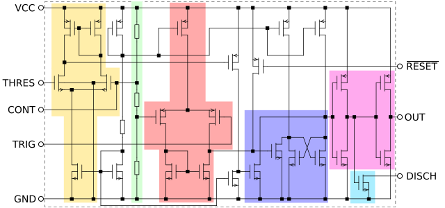
Internal schematic
The internal block diagram and schematic of the 555 timer are highlighted with the same color across all three drawings to clarify how the chip is implemented:[2]
- Voltage divider: Between the positive supply voltage VCC and the ground GND is a voltage divider consisting of three identical resistors (5 kΩ for bipolar timers, 100 kΩ or higher for CMOS) to create reference voltages for the analog comparators. CONTROL is connected between the upper two resistors, allowing an external voltage to control the reference voltages:
- When CONTROL is not driven, this divider creates an upper reference voltage of 2⁄3 VCC and a lower reference voltage of 1⁄3 VCC.
- When CONTROL is driven, the upper reference voltage will instead be VCONTROL and the lower reference voltage will be 1⁄2 VCONTROL.
- Threshold comparator: The comparator's negative input is connected to voltage divider's upper reference voltage, and the comparator's positive input is connected to THRESHOLD.
- Trigger comparator: The comparator's positive input is connected to voltage divider's lower reference, and the comparator's negative input is connected to TRIGGER.
- Latch: A set-reset latch stores the state of the timer and is controlled by the two comparators. RESET overrides the other two inputs, thus the latch (and therefore the entire timer) can be reset at any time.
- Output: The output of the latch is followed by an output stage with push–pull output drivers that can supply up to 200 mA for bipolar timers, lower for CMOS timers.
- Discharge: Also, the output of the latch controls a transistor acting as an electronic switch that connects DISCHARGE to ground.
-
![555 internal block diagram[1]](/wiki/images/thumb/1/17/NE555_Bloc_Diagram.svg/414px-NE555_Bloc_Diagram.svg.png) 555 internal block diagram[1]
555 internal block diagram[1] -
 555 internal schematic of bipolar version
 -
 555 internal schematic of CMOS version
![555 internal block diagram[1]](/wiki/File:NE555_Bloc_Diagram.svg)


Pinout
The pinout of the 8-pin 555 timer[1] and 14-pin 556 dual timer[21] are shown in the following table. Since the 556 is conceptually two 555 timers that share power pins, the pin numbers for each half are split across two columns.[2]
| 555 pin# | 556 (unit 1) | 556 (unit 2) | Pin name | Pin direction | Pin description[1][21][2] |
|---|---|---|---|---|---|
| 1 | 7 |
GND |
Power
|
Ground supply: this pin is the ground reference voltage (zero volts).[22] | |
| 2 | 6 |
8 |
TRIGGER |
Input
|
Trigger: when VTRIGGER falls below 1⁄2 VCONTROL (1⁄3 VCC, except when CONTROL is driven by an external signal), OUTPUT goes to the high state and a timing interval starts.[22] As long as TRIGGER continues to be kept at a low voltage, OUTPUT will remain in the high state. |
| 3 | 5 |
9 |
OUTPUT |
Output
|
Output: this pin is a push-pull (P.P.) output that is driven to either a low state (GND) or a high state (VCC minus approximately 1.7 volts for bipolar timers, or VCC for CMOS timers). |
| 4 | 4 |
10 |
RESET |
Input
| |
| 5 | 3 |
11 |
CONTROL |
Input
|
Control: this pin provides access to the internal voltage divider (2⁄3 VCC by default). By applying a voltage to this pin, the timing characteristics can be changed. In astable mode, this pin can be used to frequency-modulate the OUTPUT state.[16] If this pin is not used, it should be connected to a 10 nF decoupling capacitor (between this pin and GND) to ensure electrical noise doesn't affect the internal voltage divider.[2][23][22] |
| 6 | 2 |
12 |
THRESHOLD |
Input
|
Threshold: when the voltage at this pin is greater than VCONTROL (2⁄3 VCC by default except when CONTROL is driven by an external signal), then the OUTPUT high state timing interval ends, causing OUTPUT to go to the low state.[22] |
| 7 | 1 |
13 |
DISCHARGE |
Output
|
Discharge: This pin is an open-collector (O.C.) output for bipolar timers, or an open-drain (O.D.) output for CMOS timers. This pin can be used to discharge a capacitor when OUTPUT is low. In bistable latch and bistable inverter modes, this pin is unused, which allows it to be used as an alternate output.[22] |
| 8 | 14 |
VCC |
Power
|
Positive supply: For bipolar timers, the supply voltage range is typically 4.5 to 16 volts (some are spec'ed for up to 18 volts, though most will operate as low as 3 volts). For CMOS timers, the supply voltage range is typically 2 to 15 volts (some are spec'ed for up to 18 volts, and some are spec'ed as low as 1 volt). See the supply min and max columns in the derivatives table in this article. Decoupling capacitor(s) are generally applied (between this pin and GND) as a good practice.[24][23] | |
![Pinout of 555 single timer[1][2]](/wiki/File:555_Pinout.svg)
![Pinout of 556 dual timer[21][2]](/wiki/File:NE556_pennen.svg)
Modes
The 555 IC has the following operating modes:
- Astable (free-running) mode – The 555 operates as an electronic oscillator. Applications include:
- As a general-purpose oscillator or clock/periodic timer, which may be used for many things including: Light emitting diode and lamp flashers, pulse generation, pulse-width modulation (PWM), logic clocks, tone generation, security alarms, pulse-position modulation, etc.
- Analog-to-digital conversion (ADC) from an analog value represented by a resistance or capacitance into a digital pulse length.
- e.g., selecting a thermistor as timing resistor allows the use of the 555 in a temperature sensor with the period of the output pulse determined by the temperature. A microprocessor can then convert the pulse period to temperature, linearize it, and even provide calibration.
- Monostable (one-shot) mode – The 555 operates as a "one-shot" pulse generator. Applications include:
- timers, missing pulse detection, bounce-free switches, touch switches, frequency dividers, triggered measurement of resistance or capacitance, PWM, etc.
- Bistable (latch) mode – The 555 operates as a set-reset latch. Applications include:
- switch debouncing.
- Schmitt trigger (inverter) mode – the 555 operates as a Schmitt trigger inverter gate. Application:
- Converts a noisy input into a clean digital output.
Astable


| Frequency | C | R1 | R2 | Duty cycle |
|---|---|---|---|---|
| 0.1 Hz (+0.048%) | 100 μF | 8.2 kΩ | 68 kΩ | 52.8% |
| 1 Hz (+0.048%) | 10 μF | 8.2 kΩ | 68 kΩ | 52.8% |
| 10 Hz (+0.048%) | 1 μF | 8.2 kΩ | 68 kΩ | 52.8% |
| 100 Hz (+0.048%) | 100 nF | 8.2 kΩ | 68 kΩ | 52.8% |
| 1 kHz (+0.048%) | 10 nF | 8.2 kΩ | 68 kΩ | 52.8% |
| 10 kHz (+0.048%) | 1 nF | 8.2 kΩ | 68 kΩ | 52.8% |
| 100 kHz (+0.048%) | 100 pF | 8.2 kΩ | 68 kΩ | 52.8% |
In the astable configuration, the 555 timer puts out a continuous stream of rectangular pulses having a specific period.
The astable configuration is implemented using two resistors, and and one capacitor . The threshold and trigger pins are both connected to the capacitor; thus they have the same voltage.
Its repeated operating cycle (starting with the capacitor uncharged) is:
- Since the capacitor's voltage will be below 1⁄3 VCC, the trigger pin causes the 555's internal latch to change state, causing OUT to go high and the internal discharge transistor to cut-off.
- Since the discharge pin is no longer short-circuited to ground, the capacitor starts charging via current from Vcc through the resistors and .
- Once the capacitor charge reaches 2⁄3 Vcc, the threshold pin causes the 555's internal latch to change state, causing OUT to go low and the internal discharge transistor to go into saturation (maximal-conductivity) mode.
- This discharge transistor provides a discharge path, so the capacitor starts discharging through .
- Once the capacitor's voltage drops below 1⁄3 VCC, the cycle repeats from step 1.
During the first pulse, the capacitor charges from 0 V to 2⁄3 VCC, however, in later pulses, it only charges from 1⁄3 VCC to 2⁄3 VCC. Consequently, the first pulse has a longer high time interval compared to later pulses. Moreover, the capacitor charges through both resistors but only discharges through , thus the output high interval is longer than the low interval. This is shown in the following equations:
The output high time interval of each pulse is given by:[16]
The output low time interval of each pulse is given by:[16]
Hence, the frequency of the pulse is given by:[16]
and the duty cycle is given by:[16]
where is the time in seconds, is the resistance in ohms, is the capacitance in farads, and is the natural log of 2 constant.[lower-alpha 1]

Resistor requirements:
- Minimum resistance - it is recommended that 5 kiloohm be the minimum resistance for , but this doesn't mean reasonable lower values can't be used in certain applications.[2][25]
- Maximum resistance - a minimum threshold current of 0.25 microamp is required to trip the threshold comparator of a NE555 timer, thus resistance of should be limited to 6.6 megaohm when is 5 volts, or 20 megaohm when 15 volts.[2][25] If capacitor has significant leakage current, then the maximum resistance will need to be lowered to increase the charge current, otherwise will not be able to recharge the capacitor.[2][25]
Shorter duty cycle
To create an output high time shorter than the low time (i.e., a duty cycle less than 50%) a fast diode (i.e. 1N4148 signal diode) can be placed in parallel with R2, with the cathode on the capacitor side.[16] This bypasses R2 during the high part of the cycle, so that the high interval depends only on R1 and C, with an adjustment based on the voltage drop across the diode. The low time is unaffected by the diode and so remains But the diode's forward voltage drop Vdiode slows charging on the capacitor, so the high time is longer than the often-cited to become:
where Vdiode is when the diode's "on" current is 1⁄2 of VCC/R1 (which depends on the type of diode and can be found in datasheets or measured). When Vdiode is small relative to Vcc, this charging is faster and approaches but is slower the closer Vdiode is to Vcc:
As an extreme example, when VCC = 5 V, and Vdiode = 0.7 V, high time is 1.00 R1C, which is 45% longer than the "expected" 0.693 R1C. At the other extreme, when Vcc = 15 V, and Vdiode = 0.3 V, the high time is 0.725 R1C, which is closer to the expected 0.693 R1C. The equation approaches 0.693 R1C as Vdiode approaches 0 V.
Pulse-width modulation
In the previous example schematics, the control pin was not used, thus it should be connected to ground through a 10 nF decoupling capacitor to shunt electrical noise. However, if a time-varying voltage source was applied to the control pin, then the pulse widths would be modulated by the control voltage.
If pin 5 control voltage, Vc changes, thigh, tlow, frequency, and duty cycle change. The result is Pulse-width modulation. Threshold voltage is set to pin 5 control voltage, Vc. Trigger voltage is set to 1⁄2 Vc. Vc > Vcmin is a condition necessary for oscillation.
DC motor torque is proportional to current, and coil inductance dominates its electrical model. Because the isolation transistor is either saturated or cutoff, it consumes negligible power. The bulk of the power is lost in the coil resister (mechanical work 86%) and diode 14%. Note that as control voltage increases, tlow decreases, thigh, duty cycle, and inductor charge duration increases. The result is that inductor current follows control voltage limited by ripple.
-
 Voltage-controlled pulse-width modulation Waveform.
 -
 Voltage-Controlled Pulse-Width Modulation Schematic for DC Motor Torque Control


Before the first switch-mode power supply integrated circuit, 1976 SG1524,[26] and even after such chips, e.g. 1987 LT1070, were economically available in the late 1980s,[27] an early 555 use was switching-mode voltage regulator.[28][29] Timing components would be selected for duty cycle range, adequate for the current load limits. Control voltage would be the output of fixed gain amplified voltage error.
-
 Switching Mode Voltage Regulator (minimum load). With control voltage, 0.75V, duty cycle is 30%. During thigh, 13us, inductor charges 0.65A through saturated transistor. During 5.6us, inductor discharges through diode to top off capacitor. During 24us remaining in tlow, 32us, inductor is steady discharged.
 -
 Switching Mode Voltage Regulator (maximum load). With control voltage, 2.6V, duty cycle is 70%. During thigh, 68us, inductor charges 3.27mA through saturated transistor. During 32us, inductor discharges through diode to top off capacitor. No time remains in tlow, 32us, so no further load increase is supported.
 -
 Switching Mode Voltage Regulator Schematic. When Vout rises, it increases feedback transistor voltage through the resister ladder. This decreases control voltage and duty cycle to lower Vout. Vout is held with 5%, though load varies by factor of 10. The feedback capacitor introduces phase-shift to prevent feedback oscillation. Capacitor limits ripple to 1.3%. As supply voltage changes from 5V to 12V, the same duty cycle feedback loop reduces Vout change to 2V.


Monostable


Monostable mode produces an output pulse when the trigger signals drops below 1⁄3 VCC. An RC circuit sets the output pulse's duration as the time in seconds it takes to charge C to 2⁄3 VCC:[16]
where is the resistance in ohms, is the capacitance in farads, is the natural log of 3 constant.[lower-alpha 2] The output pulse duration can be lengthened or shortened as desired by adjusting the values of R and C. Subsequent triggering before the end of this timing interval will not affect the output pulse.[30]
Example values
| Time | C | R |
|---|---|---|
| 100 μs (−0.026%) | 1 nF | 91 kΩ |
| 1 ms (−0.026%) | 10 nF | 91 kΩ |
| 10 ms (−0.026%) | 100 nF | 91 kΩ |
| 100 ms (−0.026%) | 1 μF | 91 kΩ |
| 1 s (−0.026%) | 10 μF | 91 kΩ |
| 10 s (−0.026%) | 100 μF | 91 kΩ |
The timing table (right) shows common electronic component value solutions for various powers of 10 timings.
Scaling R and C by opposite powers of 10 will provide the same timing. For instance:
- 1 ms ≅ 1 nF and 910 kΩ,
- 1 ms ≅ 10 nF and 91 kΩ (values from table),
- 1 ms ≅ 100 nF and 9.1 kΩ.
For each row in the example table (right), additional timing values can easily be created by adding one to three of the same resistor value in parallel and/or series. A second resistor in parallel, the new timing is half the table time. A second resistor in series, the new timing is double the table time.
- 2.5 ms (0.25x) ≅ 100 nF and 22.75 kΩ (four 91 kΩ resistors in parallel),
- 5 ms (0.5x) ≅ 100 nF and 45.5 kΩ (two 91 kΩ resistors in parallel),
- 10 ms (1x) ≅ 100 nF and 91 kΩ (values from table),
- 15 ms (1.5x) ≅ 100 nF and 136.5 kΩ (one 91 kΩ resistor in series with "two 91 kΩ resistors in parallel"),
- 20 ms (2x) ≅ 100 nF and 182 kΩ (two 91 kΩ resistors in series),
- 25 ms (2.5x) ≅ 100 nF and 227.5 kΩ ("two 91 kΩ resistors in series" in series with "two 91 kΩ resistors in parallel"),
- 30 ms (3x) ≅ 100 nF and 273 kΩ (three 91 kΩ resistors in series),
- 40 ms (4x) ≅ 100 nF and 364 kΩ (four 91 kΩ resistors in series).
Bistable SR latch


A 555 timer can act as an active-low SR latch (though without an inverted Q output) with two outputs: output pin is a push-pull output, discharge pin is an open-collector output (requires a pull-up resistor).
For the schematic on the right, a Reset input signal connects to the RESET pin and connecting a Set input signal to the TR pin. Thus, pulling Set momentarily low acts as a "set" and transitions the output to the high state (VCC). Conversely, pulling Reset momentarily low acts as a "reset" and transitions the Out pin to the low state (GND).
No timing capacitors are required in a bistable configuration. The threshold input is grounded because it is unused.[31] The trigger and reset inputs may be held high via pull-up resistors if they are normally Hi-Z and only enabled by connecting to ground.
Bistable Schmitt trigger inverter gate


A 555 timer can be used to create a Schmitt trigger inverter gate with two outputs: output pin is a push-pull output, discharge pin is an open-collector output (requires a pull-up resistor).
For the schematic on the right, an input signal is AC-coupled through a low value series capacitor, then biased by identical high-resistance resistors and , which causes the signal to be centered at 1⁄2 Vcc. This centered signal is connected to both the trigger and threshold input pins of the timer. The input signal must be strong enough to excite the trigger levels of the comparators to exceed the lower 1⁄3 VCC and upper 2⁄3 VCC thresholds in order to cause them to change state, thus providing the Schmitt trigger feature.[32]
No timing capacitors are required in a bistable configuration.
Packages

In 1972, Signetics originally released the 555 timer in DIP-8 and TO5-8 metal can packages, and the 556 timer was released in a DIP-14 package.[4]
In 2006, the dual 556 timer was available in through-hole packages as DIP-14 (2.54 mm pitch),[21] and surface-mount packages as SO-14 (1.27 mm pitch) and SSOP-14 (0.65 mm pitch).
In 2012, the 555 was available in through-hole packages as DIP-8 (2.54 mm pitch),[33] and surface-mount packages as SO-8 (1.27 mm pitch), SSOP-8 / TSSOP-8 / VSSOP-8 (0.65 mm pitch), BGA (0.5 mm pitch).[1]
The MIC1555 is a CMOS 555-type timer with three fewer pins available in SOT23-5 (0.95 mm pitch) surface-mount package.[34]
Specifications

These specifications apply to the original bipolar NE555. Other 555 timers can have different specifications depending on the grade (industrial, military, medical, etc.).
| Part number | NE555 |
| IC Process | Bipolar |
| Supply voltage (VCC) | 4.5 to 16 V |
| Supply current (VCC = +5 V) | 3 to 6 mA |
| Supply current (VCC = +15 V) | 10 to 15 mA |
| Output current (maximum) | 200 mA |
| Maximum Power dissipation | 600 mW |
| Power consumption (minimum operating) | 30 mW @ 5 V, 225 mW @ 15 V |
| Operating temperature | 0 to 70 °C |
Derivatives
Numerous companies have manufactured one or more variants of the 555, 556, 558 timers over the past decades, under many different part numbers. The following is a partial list:
| Manufacturer | Part number |
Production status |
IC process |
Timers total |
Supply min. (volt) |
Supply max. (volt) |
Iq (μA) at 5 V supply |
Frequency max. (MHz) |
Remarks | Datasheet |
|---|---|---|---|---|---|---|---|---|---|---|
| Custom Silicon Solutions (CSS) | CSS555 | Active | CMOS | 1 | 1.2 | 5.5 | 4.3 | 1.0 | Internal EEPROM, requires programmer | [35][36][37] |
| Diodes Inc | ZSCT1555 | Discontinued | Bipolar | 1 | 0.9 | 6 | 150 | 0.33 | Designed by Hans Camenzind | [38] |
| Japan Radio Company (JRC) | NJM555 | Discontinued | Bipolar | 1 | 4.5 | 16 | 3000 | 0.1* | Also available in SIP-8 package. | [33] |
| Microchip | MIC1555/7 | Active | CMOS | 1* | 2.7 | 18 | 240 | 5.0* | Reduced pins & features (only astable & monostable & no reset for MIC1555, astable only for MIC1557), only available in SOT23-5, TSOT23-5, UTDFN-10 packages. | [34] |
| ON | MC1455 | Active | Bipolar | 1 | 4.5 | 16 | 3000 | 0.1* | — | [39] |
| Renesas | ICM7555 | Active | CMOS | 1 | 2 | 18 | 40 | 1.0 | [17] | |
| Renesas | ICM7556 | Active | CMOS | 2 | 2 | 18 | 80 | 1.0 | [17] | |
| Signetics | NE555 | Active (TI) | Bipolar | 1 | 4.5 | 16 | 3000 | 0.1* | First 555 timer, DIP-8 or TO5-8 packages. | [4][16][25][2] |
| Signetics | NE556 | Active (TI) | Bipolar | 2 | 4.5 | 16 | 6000 | 0.1* | First 556 timer, DIP-14 package. | [16][2] |
| Signetics | NE558 | Discontinued | Bipolar | 4* | 4.5 | 16 | 4800* | 0.1* | First 558 timer, DIP-16 package. | [2] |
| STMicroelectronics (ST) | TS555 | Active | CMOS | 1 | 2 | 16 | 110 | 2.7 | — | [40] |
| Texas Instruments (TI) | LM555 | Active | Bipolar | 1 | 4.5 | 16 | 3000 | unspecified | [30] | |
| Texas Instruments | LM556 | Discontinued | Bipolar | 2 | 4.5 | 16 | 6000 | 0.1 | [41] | |
| Texas Instruments | LMC555 | Active | CMOS | 1 | 1.5 | 15 | 100 | 3.0 | Also available in DSBGA-8 package. | [18] |
| Texas Instruments | NE555 | Active | Bipolar | 1 | 4.5 | 16 | 3000 | 0.1* | — | [1] |
| Texas Instruments | NE556 | Active | Bipolar | 2 | 4.5 | 16 | 6000 | 0.1* | — | [21] |
| Texas Instruments | TLC551 | Active | CMOS | 1 | 1 | 15 | 170 | 1.8 | [20] | |
| Texas Instruments | TLC552 | Active | CMOS | 2 | 1 | 15 | 340 | 1.8 | [42] | |
| Texas Instruments | TLC555 | Active | CMOS | 1 | 2 | 15 | 170 | 2.1 | — | [19] |
| Texas Instruments | TLC556 | Active | CMOS | 2 | 2 | 15 | 340 | 2.1 | — | [43] |
| X-REL | XTR655 | Active | SOI | 1 | 2.8 | 5.5 | 170 | 4.0 | Extreme (−60 °C to +230 °C), ceramic DIP-8 package or bare die. | [44] |
- Table notes
- All information in the above table was pulled from references in the datasheet column, except where denoted below.
- For the "Total timers" column, a "*" denotes parts that are missing 555 timer features.
- For the "Iq" column, a 5-volt supply was chosen as a common voltage to make it easier to compare. The value for Signetics NE558 is an estimate because NE558 datasheets don't state Iq at 5 V.[2] The value listed in this table was estimated by comparing the 5 V to 15 V ratio of other bipolar datasheets, then derating the 15 V parameter for the NE558 part, which is denoted by the "*".
- For the "Frequency max." column, a "*" denotes values that may not be the actual maximum frequency limit of the part. The MIC1555 datasheet discusses limitations from 1 to 5 MHz.[34] Though most bipolar timers don't state the maximum frequency in their datasheets, they all have a maximum frequency limitation of hundreds of kHz across their full temperature range. Section 8.1 of the Texas Instruments NE555 datasheet[1] states a value of 100 kHz, and their website shows a value of 100 kHz in timer comparison tables. Signetics App Note 170 states that most devices will oscillate up to 1 MHz; however, when considering temperature stability, it should be limited to about 500 kHz.[2] The application note from HFO mentions that at higher supply voltages the maximum power dissipation of the circuit might limit the operating frequency, as the supply current increases with frequency.[45]
- For the "Manufacturer" column, the following associates historical 555 timer manufacturers to current company names.
- Fairchild Semiconductor was sold to ON Semiconductor in 2016.[46] ON Semiconductor was founded in 1999 as a spinoff of Motorola Semiconductor Components Group.[47] The MC1455 started as a Motorola product.
- Intersil was sold to Renesas Electronics in 2017.[48] The ICM7555 and ICM7556 started as Intersil products.
- Micrel was sold to Microchip Technology in 2015.[49] The MIC1555 started as a Micrel product.
- National Semiconductor was sold to Texas Instruments in 2011.[50] The LM555 and LM556 started as a National Semiconductor products.
- Signetics was sold to Philips Semiconductor in 1975, later to NXP Semiconductors in 2006.[51]
- Zetex Semiconductors was sold to Diodes Incorporated in 2008.[52] The ZSCT1555 started as a Zetex product.[8]
556 dual timer

The dual version is called 556. It features two complete 555 timers in a 14-pin package; only the two power-supply pins are shared between the two timers.[21][16] In 2020, the bipolar version was available as the NE556,[21] and the CMOS versions were available as the Intersil ICM7556 and Texas Instruments TLC556 and TLC552. See derivatives table in this article.[17][43][42]
558 quad timer


The quad version is called 558 and has four reduced-functionality timers in a 16-pin package designed primarily for monostable multivibrator applications.[53][2] By 2014, many versions of 16-pin NE558 have become obsolete.[54]
Partial list of differences between 558 and 555 chips:[2][54]
- One VCC and one GND, similar to 556 chip.
- Four "Reset" are tied together internally to one external pin (558).
- Four "Control Voltage" are tied together internally to one external pin (558).
- Four "Triggers" are falling-edge sensitive (558), instead of level sensitive (555).
- Two resistors in the voltage divider (558), instead of three resistors (555).
- One comparator (558), instead of two comparators (555).
- Four "Output" are open-collector (O.C.) type (558), instead of push–pull (P.P.) type (555).
See also
- RC circuit
- Counter (digital)
- Operational amplifier
- List of LM-series integrated circuits
- List of linear integrated circuits
- 4000-series integrated circuits, List of 4000-series integrated circuits
- 7400-series integrated circuits, List of 7400-series integrated circuits
- Push–pull output, Open-collector/drain output, Three-state output
Notes
- ↑ ln(2) is a constant, approximately 0.693147 (rounded to 6 significant digits), or commonly rounded to fewer digits in 555 timer books and datasheets to 0.693, 0.69, or 0.7
- ↑ ln(3) is a constant, approximately 1.098612 (rounded to 6 significant digits), or commonly rounded to fewer digits in 555 timer books and datasheets to 1.099 or 1.1
References
- ↑ 1.0 1.1 1.2 1.3 1.4 1.5 1.6 1.7 1.8 "NE555 Datasheet". September 2014. http://www.ti.com/lit/ds/symlink/ne555.pdf.
- ↑ 2.00 2.01 2.02 2.03 2.04 2.05 2.06 2.07 2.08 2.09 2.10 2.11 2.12 2.13 2.14 2.15 2.16 2.17 2.18 2.19 "Linear LSI Data and Applications Manual". 1985. https://archive.org/details/bitsavers_signeticsdcsLinearLSI_66682786.
- ↑ 3.0 3.1 Fuller, Brian (15 August 2012). "Hans Camenzind, 555 timer inventor, dies". EE Times. http://www.eetimes.com/document.asp?doc_id=1262353.
- ↑ 4.0 4.1 4.2 "Linear Vol1 Databook". 1972. https://archive.org/details/bitsavers_signeticsdcsLinearVol1_11470058.
- ↑ Lowe, Doug (2017-02-06). Electronics All-in-One For Dummies. Wiley. pp. 339. ISBN 978-1-119-32079-1. https://books.google.com/books?id=Ivn-DQAAQBAJ&pg=PA339. "The 555 timer chip, developed in 1970, is probably the most popular integrated circuit ever made. By some estimates, more than a billion of them are manufactured every year."
- ↑ 6.0 6.1 Carmenzind, Hans (2010). "タイマIC 555 誕生秘話" (in ja). トランジスタ技術 (CQ出版) 47 (12): 73, 74. ISSN 0040-9413.
- ↑ Santo, Brian (May 2009). "25 Microchips That Shook the World". IEEE Spectrum 46 (5): 34–43. doi:10.1109/MSPEC.2009.4907384. https://spectrum.ieee.org/25-microchips-that-shook-the-world.
- ↑ 8.0 8.1 8.2 8.3 8.4 Camenzind, H.R. (September 1997). "Redesigning the old 555 [timer circuit]". IEEE Spectrum 34 (9): 80–85. doi:10.1109/6.619384.
- ↑ Ward, Jack (2004). "The 555 Timer IC – An Interview with Hans Camenzind". The Semiconductor Museum. http://www.semiconductormuseum.com/Transistors/LectureHall/Camenzind/Camenzind_Index.htm.
- ↑ Scherz, Paul; Monk, Simon (2016). Practical Electronics for Inventors (4th ed.). McGraw Hill. pp. 687. ISBN 978-1-259-58755-9. https://books.google.com/books?id=lhSCCwAAQBAJ. "The 555 gets its name from the three 5-kW +VCC R1 discharging path 555 R 2 C 6 resistors shown in the block diagram. These resistors act as a three-step voltage."
- ↑ Kleitz, William (1990). Digital electronics : a practical approach (2nd ed.). Prentice Hall. pp. 401. ISBN 0-13-211657-X. OCLC 20218185. "The 555 got its name from the three 5-kOhm resistors"
- ↑ Simpson, Colin D. (1996). Industrial electronics. Prentice Hall. pp. 357. ISBN 0-02-410622-4. OCLC 33014077. "The reference voltage for the comparators is established by a voltage divider consisting of three 5 - k2 resistors, which is where the name 555 is derived"
- ↑ GoldStein, Harry (March 3, 2003). "The Irresistible Transistor". IEEE Spectrum 40 (3): 42–47. doi:10.1109/MSPEC.2003.1184435. https://spectrum.ieee.org/the-irresistible-transistor. Retrieved 2020-08-29.
- ↑ "Oral History Hans Camenzind Historic 555 IC Page2". The Semiconductor Museum. http://www.semiconductormuseum.com/Transistors/LectureHall/Camenzind/Camenzind_Page2.htm.
- ↑ "Oral History Hans Camenzind Historic 555 Integrated Circuit Page6". http://www.semiconductormuseum.com/Transistors/LectureHall/Camenzind/Camenzind_Page6.htm.
- ↑ 16.00 16.01 16.02 16.03 16.04 16.05 16.06 16.07 16.08 16.09 16.10 16.11 "555/556 Timers Databook". 1973. https://www.rfcafe.com/miscellany/cool-products/Signetics-555-556-Timer-1973-Databook.pdf.
- ↑ 17.0 17.1 17.2 17.3 "ICM7555-556 Datasheet". June 2016. http://www.intersil.com/content/dam/Intersil/documents/icm7/icm7555-56.pdf.
- ↑ 18.0 18.1 "LMC555 Datasheet". July 2016. http://www.ti.com/lit/ds/symlink/lmc555.pdf.
- ↑ 19.0 19.1 "TLC555 Datasheet". August 2016. http://www.ti.com/lit/ds/symlink/tlc555.pdf.
- ↑ 20.0 20.1 "TLC551 Datasheet". September 1997. http://www.ti.com/lit/ds/symlink/tlc551.pdf.
- ↑ 21.0 21.1 21.2 21.3 21.4 21.5 21.6 21.7 "NE556 Datasheet". June 2006. http://www.ti.com/lit/ds/symlink/ne556.pdf.
- ↑ 22.0 22.1 22.2 22.3 22.4 Cite error: Invalid
<ref>tag; no text was provided for refs namedBook-IC-Timer-Cookbook - ↑ 23.0 23.1 Cite error: Invalid
<ref>tag; no text was provided for refs namedBook-TTL-Cookbook - ↑ Carr, Joseph (1996-12-19) (in en). Linear IC Applications: A Designer's Handbook. Newnes. pp. 119. ISBN 978-0-7506-3370-3. https://books.google.com/books?id=DyX_dKLyZVwC&q=555+%22decoupling+capacitor%22&pg=PA119.
- ↑ 25.0 25.1 25.2 25.3 "Analog Applications Manual". 1979. https://archive.org/details/bitsavers_signeticsdcsAnalogApplications_33415016.
- ↑ Shirriff, Ken (August 2019). "The Quiet Remaking of Computer Power Supplies". IEEE Spectrum. https://spectrum.ieee.org/a-half-century-ago-better-transistors-and-switching-regulators-revolutionized-the-design-of-computer-power-supplies.
- ↑ Jim, Williams. "(Application Note 25: Switching Regulators for Poets A Gentle Guide for the Trepidatious". Analog Devices nee Linear Technologies. https://www.analog.com/media/en/technical-documentation/application-notes/an25fa.pdf.
- ↑ "The History of 555 Timer IC – Story of Invention by Hans Camenzind:555 timer IC as a PWM generator". Circuits Today 2026. https://circuitstoday.com/the-history-555-timer-ic.
- ↑ "Re: Any experience designing 555 switched mode power supplies?". DIYstompboxes.com. January 11, 2009. p. Reply #2. https://www.diystompboxes.com/smfforum/index.php?msg=595298. "Using a 555 for a switched mode power supply is how we (= us EE power supply designers, at the time) used to do things before there were custom chips for this."
- ↑ 30.0 30.1 "LM555 Datasheet". January 2015. http://www.ti.com/lit/ds/symlink/lm555.pdf.
- ↑ Buiting, Jan (2003) (in en). 308 Circuits. Elektor International Media. ISBN 978-0-905705-66-8. https://books.google.com/books?id=rZDbnQ0siCYC&q=555+pin+7+%22open+collector%22&pg=PA84.
- ↑ "555 Timer as Schmitt Trigger". June 19, 2015. https://www.electronicshub.org/555-timer-as-schmitt-trigger/.
- ↑ 33.0 33.1 "NJM555 Datasheet". November 2012. http://www.njr.com/semicon/PDF/NJM555_E.pdf.
- ↑ 34.0 34.1 34.2 "MIC1555 Datasheet". March 2017. http://ww1.microchip.com/downloads/en/DeviceDoc/20005730A.pdf.
- ↑ "CSS555 Datasheet". July 2012. http://www.customsiliconsolutions.com/downloads/Revised%20Standard%20products/CSS555_Spec_2.pdf.
- ↑ "CSS555 Part Search". https://www.jameco.com/shop/StoreCatalogDrillDownView?langId=-1&storeId=10001&catalogId=10001&freeText=css555&search_type=jamecoall.
- ↑ Senft, James (February 2016). "The Remarkable CSS555". Nuts & Volts Magazine. https://www.nutsvolts.com/magazine/article/february2016_CSS555TimerICs.
- ↑ "ZSCT1555 Datasheet". July 2006. https://www.diodes.com/assets/Datasheets/ZSCT1555.pdf.
- ↑ "MC1455 Datasheet". December 2009. https://www.onsemi.com/pub/Collateral/MC1455-D.PDF.
- ↑ "TS555 Datasheet". June 2015. https://www.st.com/resource/en/datasheet/ts555.pdf.
- ↑ "LM556 Datasheet". October 2015. http://www.ti.com/lit/ds/symlink/lm556.pdf.
- ↑ 42.0 42.1 "TLC552 Datasheet". May 1988. http://www.ti.com/lit/ds/symlink/tlc552.pdf.
- ↑ 43.0 43.1 "TLC556 Datasheet". September 1997. http://www.ti.com/lit/ds/symlink/tlc556.pdf.
- ↑ "XTR655 Datasheet". August 2021. https://www.easii-ic.com/wp-content/uploads/2021/08/EASii-IC-DS-XTR650-Versatile-Timer-Rev-3-August-21-DS-00100-11.pdf.
- ↑ Reick, Ullrich (1986-03-01) (in de). Zeitgeber-IS B 555 / B 556. Halbleiterwerk Frankfurt (Oder). http://datasheet.datasheetarchive.com/originals/scans/Scans-048/DSAGER000125.pdf.
- ↑ "ON Semiconductor Successfully Completes Acquisition of Fairchild Semiconductor". September 19, 2016. https://www.businesswire.com/news/home/20160919005796/en/Semiconductor-Successfully-Completes-Acquisition-Fairchild-Semiconductor-2.4.
- ↑ "Former Motorola group emerges as ON Semiconductor". EE Times. August 5, 1999. https://www.eetimes.com/former-motorola-group-emerges-as-on-semiconductor/#.
- ↑ "Renesas and Intersil Announce Final Regulatory Approval for Renesas' Acquisition of Intersil". February 22, 2017. https://www.renesas.com/us/en/about/press-center/news/2017/news20170222.html.
- ↑ "Microchip Technology Completes Micrel Acquisition". August 12, 2015. https://www.powerelectronics.com/news/industry/article/21862805/microchip-technology-completes-micrel-acquisition.
- ↑ "Texas Instruments completes acquisition of National Semiconductor". September 23, 2011. https://investor.ti.com/news-releases/news-release-details/texas-instruments-completes-acquisition-national-semiconductor.
- ↑ "NXP Semiconductors history". 2008. https://www.siliconvalleyhistorical.org/nxp-semiconductors-history.
- ↑ "Diodes Incorporated closes acquisition of Zetex". June 13, 2008. https://www.ledsmagazine.com/leds-ssl-design/driver-ics/article/16697918/diodes-incorporated-closes-acquisition-of-zetex-plc.
- ↑ Horn, Delton (1994). Amplifiers, waveform generators, and other low-cost IC projects. New York: TAB Books. pp. 27. ISBN 0-07-030415-7. OCLC 28676554. "Not all functions are brought out to the 558's pins. This chip is designed primarily for monostable multivibrator applications"
- ↑ 54.0 54.1 Platt, Charles; Jansson, Fredrik (2014-11-13) (in en). LEDs, LCDs, Audio, Thyristors, Digital Logic, and Amplification. Encyclopedia of Electronic Components. 2. Maker Media. ISBN 978-1-4493-3414-7. https://books.google.com/books?id=FgRYBQAAQBAJ&pg=PT213.
Further reading
- Books
- 555 Timer Applications Sourcebook With Experiments; 2nd Ed; Howard Berlin; BPB Publications; 218 pages; 2008; ISBN 978-8176567909. (1st Ed in 1978)
- Timer/Generator Circuits Manual; 1st Ed; R.M. Marston; Newnes; 276 pages; 1990; ISBN 978-0434912919.
- Engineer's Mini-Notebook – 555 Timer IC Circuits; 3rd Ed; Forrest Mims III; Radio Shack; 33 pages; 1989; ASIN B000MN54A6. (1st Ed in 1984)
- IC Timer Cookbook; 2nd Ed; Walt Jung; Sams Publishing; 384 pages; 1983; ISBN 978-0672219320. (1st Ed in 1977)
- 110 IC Timer Projects; Jules Gilder; Hayden; 115 pages; 1979; ISBN 978-0810456884.
- IC 555 Projects; E.A. Parr; Bernard Babani Publishing; 144 pages; 1978; ISBN 978-0859340472.
- Books with timer chapters
- Lessons in Electric Circuits - Volume VI - Experiments; Tony Kuphaldt; Open Book Project; 423 pages; 2010. (Chapter 6 and 8)
- Designing Analog Chips; Hans Camenzind (inventor of 555 timer); Virtual Bookworm; 244 pages; 2005; ISBN 978-1589397187. (Chapter 11)
- Timer, Op Amp, and Optoelectronic Circuits and Projects; Forrest Mims III; Master Publishing; 128 pages; 2004; ISBN 978-0945053293. (Chapter 1)
- Linear LSI Data and Applications Manual; Signetics; 1250 pages; 1985. (Appnotes AN170/171 and Datasheets NE555/6/8)
- Analog Applications Manual; Signetics; 418 pages; 1979. (Chapter 6)
- TTL Cookbook; Don Lancaster; Sams Publishing; 412 pages; 1974; ISBN 978-0672210358. (Chapter 4, pages 171-188)
- Datasheets
- See links in "Derivatives" table and "References" section in this article.
External links
- Using the 555 Timer IC in Special or Unusual Circuits - Nuts & Volts magazine
- 555 Timer Tutorial - Tony van Roon
- Common Mistakes When Using a 555 Timer
- 555 timing calculators: astable, monostable
- Teardown of a bipolar RCA LM555CH chip
- Teardown of a CMOS TI LMC555 chip
 |  |

