Engineering:Sensor
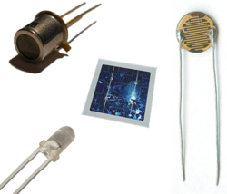
A sensor is a device that produces an output signal for the purpose of sensing a physical phenomenon.
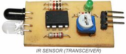
In the broadest definition, a sensor is a device, module, machine, or subsystem that detects events or changes in its environment and sends the information to other electronics, frequently a computer processor.
Sensors are used in everyday objects such as touch-sensitive elevator buttons (tactile sensor) and lamps which dim or brighten by touching the base, and in innumerable applications of which most people are never aware. With advances in micromachinery and easy-to-use microcontroller platforms, the uses of sensors have expanded beyond the traditional fields of temperature, pressure and flow measurement,[1] for example into MARG sensors.
Analog sensors such as potentiometers and force-sensing resistors are still widely used. Their applications include manufacturing and machinery, airplanes and aerospace, cars, medicine, robotics and many other aspects of our day-to-day life. There is a wide range of other sensors that measure chemical and physical properties of materials, including optical sensors for refractive index measurement, vibrational sensors for fluid viscosity measurement, and electro-chemical sensors for monitoring pH of fluids.
A sensor's sensitivity indicates how much its output changes when the input quantity it measures changes. For instance, if the mercury in a thermometer moves 1 cm when the temperature changes by 1 °C, its sensitivity is 1 cm/°C (it is basically the slope dy/dx assuming a linear characteristic). Some sensors can also affect what they measure; for instance, a room temperature thermometer inserted into a hot cup of liquid cools the liquid while the liquid heats the thermometer. Sensors are usually designed to have a small effect on what is measured; making the sensor smaller often improves this and may introduce other advantages.[2]
Technological progress allows more and more sensors to be manufactured on a microscopic scale as microsensors using MEMS technology. In most cases, a microsensor reaches a significantly faster measurement time and higher sensitivity compared with macroscopic approaches.[2][3] Due to the increasing demand for rapid, affordable and reliable information in today's world, disposable sensors—low-cost and easy‐to‐use devices for short‐term monitoring or single‐shot measurements—have recently gained growing importance. Using this class of sensors, critical analytical information can be obtained by anyone, anywhere and at any time, without the need for recalibration and worrying about contamination.[4]
Classification of measurement errors
A good sensor obeys the following rules:[4]
- it is sensitive to the measured property
- it is insensitive to any other property likely to be encountered in its application, and
- it does not influence the measured property.
Most sensors have a linear transfer function. The sensitivity is then defined as the ratio between the output signal and measured property. For example, if a sensor measures temperature and has a voltage output, the sensitivity is constant with the units [V/K]. The sensitivity is the slope of the transfer function. Converting the sensor's electrical output (for example V) to the measured units (for example K) requires dividing the electrical output by the slope (or multiplying by its reciprocal). In addition, an offset is frequently added or subtracted. For example, −40 must be added to the output if 0 V output corresponds to −40 C input.
For an analog sensor signal to be processed or used in digital equipment, it needs to be converted to a digital signal, using an analog-to-digital converter.
Sensor deviations
Since sensors cannot replicate an ideal transfer function, several types of deviations can occur which limit sensor accuracy:
- Since the range of the output signal is always limited, the output signal will eventually reach a minimum or maximum when the measured property exceeds the limits. The full scale range defines the maximum and minimum values of the measured property. [citation needed]
- The sensitivity may in practice differ from the value specified. This is called a sensitivity error. This is an error in the slope of a linear transfer function.
- If the output signal differs from the correct value by a constant, the sensor has an offset error or bias. This is an error in the y-intercept of a linear transfer function.
- Nonlinearity is deviation of a sensor's transfer function from a straight line transfer function. Usually, this is defined by the amount the output differs from ideal behavior over the full range of the sensor, often noted as a percentage of the full range.
- Deviation caused by rapid changes of the measured property over time is a dynamic error. Often, this behavior is described with a bode plot showing sensitivity error and phase shift as a function of the frequency of a periodic input signal.
- If the output signal slowly changes independent of the measured property, this is defined as drift. Long term drift over months or years is caused by physical changes in the sensor.
- Noise is a random deviation of the signal that varies in time.
- A hysteresis error causes the output value to vary depending on the previous input values. If a sensor's output is different depending on whether a specific input value was reached by increasing vs. decreasing the input, then the sensor has a hysteresis error.
- If the sensor has a digital output, the output is essentially an approximation of the measured property. This error is also called quantization error.
- If the signal is monitored digitally, the sampling frequency can cause a dynamic error, or if the input variable or added noise changes periodically at a frequency near a multiple of the sampling rate, aliasing errors may occur.
- The sensor may to some extent be sensitive to properties other than the property being measured. For example, most sensors are influenced by the temperature of their environment.
All these deviations can be classified as systematic errors or random errors. Systematic errors can sometimes be compensated for by means of some kind of calibration strategy. Noise is a random error that can be reduced by signal processing, such as filtering, usually at the expense of the dynamic behavior of the sensor.
Resolution
The sensor resolution or measurement resolution is the smallest change that can be detected in the quantity that is being measured. The resolution of a sensor with a digital output is usually the numerical resolution of the digital output. The resolution is related to the precision with which the measurement is made, but they are not the same thing. A sensor's accuracy may be considerably worse than its resolution.
- For example, the distance resolution is the minimum distance that can be accurately measured by any distance measuring devices. In a time-of-flight camera, the distance resolution is usually equal to the standard deviation (total noise) of the signal expressed in unit of length.
- The sensor may to some extent be sensitive to properties other than the property being measured. For example, most sensors are influenced by the temperature of their environment.
Chemical sensor
A chemical sensor is a self-contained analytical device that can provide information about the chemical composition of its environment, that is, a liquid or a gas phase.[5][6] The information is provided in the form of a measurable physical signal that is correlated with the concentration of a certain chemical species (termed as analyte). Two main steps are involved in the functioning of a chemical sensor, namely, recognition and transduction. In the recognition step, analyte molecules interact selectively with receptor molecules or sites included in the structure of the recognition element of the sensor. Consequently, a characteristic physical parameter varies and this variation is reported by means of an integrated transducer that generates the output signal. A chemical sensor based on recognition material of biological nature is a biosensor. However, as synthetic biomimetic materials are going to substitute to some extent recognition biomaterials, a sharp distinction between a biosensor and a standard chemical sensor is superfluous. Typical biomimetic materials used in sensor development are molecularly imprinted polymers and aptamers.[7]
Biosensor
In biomedicine and biotechnology, sensors which detect analytes thanks to a biological component, such as cells, protein, nucleic acid or biomimetic polymers, are called biosensors. Whereas a non-biological sensor, even organic (carbon chemistry), for biological analytes is referred to as sensor or nanosensor. This terminology applies for both in-vitro and in vivo applications. The encapsulation of the biological component in biosensors, presents a slightly different problem that ordinary sensors; this can either be done by means of a semipermeable barrier, such as a dialysis membrane or a hydrogel, or a 3D polymer matrix, which either physically constrains the sensing macromolecule or chemically constrains the macromolecule by bounding it to the scaffold.
Neuromorphic sensors
Neuromorphic sensors are sensors that physically mimic structures and functions of biological neural entities.[8] One example of this is the event camera.
MOS sensors
Metal–oxide–semiconductor (MOS) technology originates from the MOSFET (MOS field-effect transistor, or MOS transistor) invented by Mohamed M. Atalla and Dawon Kahng in 1959, and demonstrated in 1960.[9] MOSFET sensors (MOS sensors) were later developed, and they have since been widely used to measure physical, chemical, biological and environmental parameters.[10]
Biochemical sensors
A number of MOSFET sensors have been developed, for measuring physical, chemical, biological, and environmental parameters.[10] The earliest MOSFET sensors include the open-gate field-effect transistor (OGFET) introduced by Johannessen in 1970,[10] the ion-sensitive field-effect transistor (ISFET) invented by Piet Bergveld in 1970,[11] the adsorption FET (ADFET) patented by P.F. Cox in 1974, and a hydrogen-sensitive MOSFET demonstrated by I. Lundstrom, M.S. Shivaraman, C.S. Svenson and L. Lundkvist in 1975.[10] The ISFET is a special type of MOSFET with a gate at a certain distance,[10] and where the metal gate is replaced by an ion-sensitive membrane, electrolyte solution and reference electrode.[12] The ISFET is widely used in biomedical applications, such as the detection of DNA hybridization, biomarker detection from blood, antibody detection, glucose measurement, pH sensing, and genetic technology.[12]
By the mid-1980s, numerous other MOSFET sensors had been developed, including the gas sensor FET (GASFET), surface accessible FET (SAFET), charge flow transistor (CFT), pressure sensor FET (PRESSFET), chemical field-effect transistor (ChemFET), reference ISFET (REFET), biosensor FET (BioFET), enzyme-modified FET (ENFET) and immunologically modified FET (IMFET).[10] By the early 2000s, BioFET types such as the DNA field-effect transistor (DNAFET), gene-modified FET (GenFET) and cell-potential BioFET (CPFET) had been developed.[12]
Image sensors
MOS technology is the basis for modern image sensors, including the charge-coupled device (CCD) and the CMOS active-pixel sensor (CMOS sensor), used in digital imaging and digital cameras.[13] Willard Boyle and George E. Smith developed the CCD in 1969. While researching the MOS process, they realized that an electric charge was the analogy of the magnetic bubble and that it could be stored on a tiny MOS capacitor. As it was fairly straightforward to fabricate a series of MOS capacitors in a row, they connected a suitable voltage to them so that the charge could be stepped along from one to the next.[13] The CCD is a semiconductor circuit that was later used in the first digital video cameras for television broadcasting.[14]
The MOS active-pixel sensor (APS) was developed by Tsutomu Nakamura at Olympus in 1985.[15] The CMOS active-pixel sensor was later developed by Eric Fossum and his team in the early 1990s.[16]
MOS image sensors are widely used in optical mouse technology. The first optical mouse, invented by Richard F. Lyon at Xerox in 1980, used a 5 µm NMOS sensor chip.[17][18] Since the first commercial optical mouse, the IntelliMouse introduced in 1999, most optical mouse devices use CMOS sensors.[19]
Monitoring sensors

MOS monitoring sensors are used for house monitoring, office and agriculture monitoring, traffic monitoring (including car speed, traffic jams, and traffic accidents), weather monitoring (such as for rain, wind, lightning and storms), defense monitoring, and monitoring temperature, humidity, air pollution, fire, health, security and lighting.[21] MOS gas detector sensors are used to detect carbon monoxide, sulfur dioxide, hydrogen sulfide, ammonia, and other gas substances.[22] Other MOS sensors include intelligent sensors[23] and wireless sensor network (WSN) technology.[24]
See also
References
- ↑ Bennett, S. (1993). A History of Control Engineering 1930–1955. London: Peter Peregrinus Ltd. on behalf of the Institution of Electrical Engineers. ISBN 978-0-86341-280-6The source states "controls" rather than "sensors", so its applicability is assumed. Many units are derived from the basic measurements to which it refers, such as a liquid's level measured by a differential pressure sensor.
- ↑ 2.0 2.1 Jihong Yan (2015). Machinery Prognostics and Prognosis Oriented Maintenance Management. Wiley & Sons Singapore Pte. Ltd. p. 107. ISBN 9781118638729. https://books.google.com/books?id=LbzlBQAAQBAJ&pg=PA107.
- ↑ Ganesh Kumar (September 2010). Modern General Knowledge. Upkar Prakashan. p. 194. ISBN 978-81-7482-180-5. https://books.google.com/books?id=DbnFSqKSVb0C&pg=PA194.
- ↑ 4.0 4.1 Dincer, Can; Bruch, Richard; Costa‐Rama, Estefanía; Fernández‐Abedul, Maria Teresa; Merkoçi, Arben; Manz, Andreas; Urban, Gerald Anton; Güder, Firat (2019-05-15). "Disposable Sensors in Diagnostics, Food, and Environmental Monitoring" (in en). Advanced Materials 31 (30): 1806739. doi:10.1002/adma.201806739. ISSN 0935-9648. PMID 31094032.
- ↑ Toniolo, Rosanna; Dossi, Nicolò; Giannilivigni, Emanuele; Fattori, Andrea; Svigelj, Rossella; Bontempelli, Gino; Giacomino, Agnese; Daniele, Salvatore (3 March 2020). "Modified Screen Printed Electrode Suitable for Electrochemical Measurements in Gas Phase". Analytical Chemistry 92 (5): 3689–3696. doi:10.1021/acs.analchem.9b04818. ISSN 0003-2700. PMID 32008321. https://pubs.acs.org/doi/10.1021/acs.analchem.9b04818.
- ↑ Bǎnicǎ, Florinel-Gabriel (2012). Chemical Sensors and Biosensors:Fundamentals and Applications. Chichester, UK: John Wiley & Sons. p. 576. ISBN 978-1-118-35423-0.
- ↑ Svigelj, Rossella; Dossi, Nicolo; Pizzolato, Stefania; Toniolo, Rosanna; Miranda-Castro, Rebeca; de-los-Santos-Álvarez, Noemí; Lobo-Castañón, María Jesús (1 October 2020). "Truncated aptamers as selective receptors in a gluten sensor supporting direct measurement in a deep eutectic solvent". Biosensors and Bioelectronics 165: 112339. doi:10.1016/j.bios.2020.112339. PMID 32729482.
- ↑ Vanarse, Anup; Osseiran, Adam; Rassau, Alexander (2016). "A Review of Current Neuromorphic Approaches for Vision, Auditory, and Olfactory Sensors". Frontiers in Neuroscience 10: 115. doi:10.3389/fnins.2016.00115. PMID 27065784.
- ↑ "1960: Metal Oxide Semiconductor (MOS) Transistor Demonstrated". The Silicon Engine: A Timeline of Semiconductors in Computers (Computer History Museum). https://www.computerhistory.org/siliconengine/metal-oxide-semiconductor-mos-transistor-demonstrated/. Retrieved August 31, 2019.
- ↑ 10.0 10.1 10.2 10.3 10.4 10.5 Bergveld, Piet (October 1985). "The impact of MOSFET-based sensors". Sensors and Actuators 8 (2): 109–127. doi:10.1016/0250-6874(85)87009-8. ISSN 0250-6874. Bibcode: 1985SeAc....8..109B. https://core.ac.uk/download/pdf/11473091.pdf.
- ↑ Chris Toumazou; Pantelis Georgiou (December 2011). "40 years of ISFET technology: From neuronal sensing to DNA sequencing". Electronics Letters. https://www.researchgate.net/publication/260616066. Retrieved 13 May 2016.
- ↑ 12.0 12.1 12.2 Schöning, Michael J.; Poghossian, Arshak (10 September 2002). "Recent advances in biologically sensitive field-effect transistors (BioFETs)". Analyst 127 (9): 1137–1151. doi:10.1039/B204444G. ISSN 1364-5528. PMID 12375833. Bibcode: 2002Ana...127.1137S. http://juser.fz-juelich.de/record/16078/files/12968.pdf.
- ↑ 13.0 13.1 Williams, J. B. (2017). The Electronics Revolution: Inventing the Future. Springer. pp. 245 & 249. ISBN 9783319490885. https://books.google.com/books?id=v4QlDwAAQBAJ&pg=PA245.
- ↑ Boyle, William S; Smith, George E. (1970). "Charge Coupled Semiconductor Devices". Bell Syst. Tech. J. 49 (4): 587–593. doi:10.1002/j.1538-7305.1970.tb01790.x.
- ↑ Matsumoto, Kazuya et al. (1985). "A new MOS phototransistor operating in a non-destructive readout mode". Japanese Journal of Applied Physics 24 (5A): L323. doi:10.1143/JJAP.24.L323. Bibcode: 1985JaJAP..24L.323M.
- ↑ Eric R. Fossum (1993), "Active Pixel Sensors: Are CCD's Dinosaurs?" Proc. SPIE Vol. 1900, p. 2–14, Charge-Coupled Devices and Solid State Optical Sensors III, Morley M. Blouke; Ed.
- ↑ Lyon, Richard F. (2014). "The Optical Mouse: Early Biomimetic Embedded Vision". Advances in Embedded Computer Vision. Springer. pp. 3–22 (3). ISBN 9783319093871. https://books.google.com/books?id=p_GbBQAAQBAJ&pg=PA3.
- ↑ Lyon, Richard F. (August 1981). "The Optical Mouse, and an Architectural Methodology for Smart Digital Sensors". VLSI Systems and Computations. Computer Science Press. pp. 1–19. doi:10.1007/978-3-642-68402-9_1. ISBN 978-3-642-68404-3. http://bitsavers.trailing-edge.com/pdf/xerox/parc/techReports/VLSI-81-1_The_Optical_Mouse.pdf.
- ↑ Brain, Marshall; Carmack, Carmen (24 April 2000). "How Computer Mice Work" (in en). https://computer.howstuffworks.com/mouse4.htm.
- ↑ "LiDAR vs. 3D ToF Sensors — How Apple Is Making AR Better for Smartphones". https://ios.gadgethacks.com/news/lidar-vs-3d-tof-sensors-apple-is-making-ar-better-for-smartphones-0280778/.
- ↑ Omura, Yasuhisa; Mallik, Abhijit; Matsuo, Naoto (2017). MOS Devices for Low-Voltage and Low-Energy Applications. John Wiley & Sons. pp. 3–4. ISBN 9781119107354. https://books.google.com/books?id=yOjFDQAAQBAJ&pg=PA3.
- ↑ Sun, Jianhai; Geng, Zhaoxin; Xue, Ning; Liu, Chunxiu; Ma, Tianjun (17 August 2018). "A Mini-System Integrated with Metal-Oxide-Semiconductor Sensor and Micro-Packed Gas Chromatographic Column". Micromachines 9 (8): 408. doi:10.3390/mi9080408. ISSN 2072-666X. PMID 30424341.
- ↑ Analog VLSI Implementation of Neural Systems. The Kluwer International Series in Engineering and Computer Science. 80. Norwell, MA: Kluwer Academic Publishers. May 8, 1989. doi:10.1007/978-1-4613-1639-8. ISBN 978-1-4613-1639-8. http://fennetic.net/irc/Christopher%20R.%20Carroll%20Carver%20Mead%20Mohammed%20Ismail%20Analog%20VLSI%20Implementation%20of%20Neural%20Systems.pdf.
- ↑ Oliveira, Joao; Goes, João (2012). Parametric Analog Signal Amplification Applied to Nanoscale CMOS Technologies. Springer Science & Business Media. p. 7. ISBN 9781461416708. https://books.google.com/books?id=Ahl_OuKxsToC&pg=PR7.
Further reading
- M. Kretschmar and S. Welsby (2005), Capacitive and Inductive Displacement Sensors, in Sensor Technology Handbook, J. Wilson editor, Newnes: Burlington, MA.
- C. A. Grimes, E. C. Dickey, and M. V. Pishko (2006), Encyclopedia of Sensors (10-Volume Set), American Scientific Publishers. ISBN:1-58883-056-X
- Blaauw, F.J., Schenk, H.M., Jeronimus, B.F., van der Krieke, L., de Jonge, P., Aiello, M., Emerencia, A.C. (2016). Let’s get Physiqual – An intuitive and generic method to combine sensor technology with ecological momentary assessments. Journal of Biomedical Informatics, vol. 63, page 141–149.
- http://www.cbm-sweden.se/images/Seminarie/Class_Descriptions_IDA_MEMS.pdf (see https://web.archive.org/web/20160304105724/http://www.cbm-sweden.se/images/Seminarie/Class_Descriptions_IDA_MEMS.pdf)
 |


