Engineering:Xenos (graphics chip)

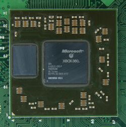
The Xenos is a custom graphics processing unit (GPU) designed by ATI (now taken over by AMD), used in the Xbox 360 video game console developed and produced for Microsoft. Developed under the codename "C1",[1] it is in many ways related to the R520 architecture and therefore very similar to an ATI Radeon X1800 XT series of PC graphics cards as far as features and performance are concerned. However, the Xenos introduced new design ideas that were later adopted in the TeraScale microarchitecture, such as the unified shader architecture.[2] The package contains two separate dies, the GPU and an eDRAM (manufactured by NEC), featuring a total of 337 million transistors.
Specifications
The TeraScale microarchitecture is based on this chip, the shader units are organized in three SIMD groups with 16 processors per group, for a total of 48 processors. Each of these processors is composed of a 5-wide vector unit (total 5 FP32 ALUs), resulting in 240 units, that can serially execute up to two instructions per cycle (a multiply and an addition). All processors in a SIMD group execute the same instruction, so in total up to three instruction threads can be simultaneously under execution.
- 500 MHz parent GPU on 90 nm, 65 nm (since 2008) TSMC process or 45 nm GlobalFoundries process (since 2010, with CPU on same die) of total 232 million transistors
- 240 vector units floating-point vector processors for shader execution, divided in three dynamically scheduled SIMD groups of 80 units each.[3]
- Unified shading architecture (each pipeline is capable of running either pixel or vertex shaders)
- 10 FP ops per vector processor per cycle (5 fused multiply-add)
- Maximum vertex count: 1.21 billion vertices per second
- Maximum polygon count: ~500 million polygons per second
- Maximum shader operations: 240 billion shader operations per second (3 shader pipelines × 80 units × 2 ALUs × 0.5 GHz (500 MHz))
- 240 GFLOPS
- MEMEXPORT shader function
- 16 texture filtering units (TF) and 16 texture addressing units (TA)
- Maximum dot product operations: 24 billion per second
- Support for a superset of DirectX 9.0c API DirectX Xbox 360, and Shader Model 3.0+
- 240 vector units floating-point vector processors for shader execution, divided in three dynamically scheduled SIMD groups of 80 units each.[3]
- 500 MHz, 10 MB daughter embedded DRAM framebuffer (at 256 Gbit/s) on 90 nm, 80 nm (since 2008)[4] or 65 nm (since 2010)[5]
- NEC designed eDRAM die includes additional logic (192 parallel pixel processors) for color, alpha compositing, alpha blending, Z/stencil buffering, and anti-aliasing called "Intelligent Memory", giving developers 4-sample anti-aliasing at very little performance cost.
- Procedural Synthesis Technology (XPS): During read streaming into the CPU, a custom prefetch instruction, extended data cache block touch (xDCBT) prefetches data directly to the L1 data cache of the intended core, which skips putting the data in the L2 cache to avoid thrashing the L2 cache. Writes streaming from each core skip the L1 cache, due to its no-write allocation (avoids thrashing of high-bandwidth, transient, write-only data streams on the L1 cache), and goes directly to the L2 cache. The system allows for the GPU to directly read data produced by the CPU without going to main memory. In this specific case of data streaming, called Xbox procedural synthesis (XPS), the CPU is effectively a data decompressor, generating geometry on-the-fly for consumption by the GPU 3D core.
- 105 million transistors[6]
- 8 render output units
- Maximum pixel fillrate: 16 gigasamples per second fillrate using 4X multisample anti aliasing (MSAA), or 32 gigasamples using Z-only operation; 4 gigapixels per second without MSAA (8 ROPs × 500 MHz)
- Maximum Z sample rate: 8 gigasamples per second (2 Z samples × 8 ROPs × 500 MHz), 32 gigasamples per second using 4X anti aliasing (2 Z samples × 8 ROPs × 4X AA × 500 MHz)[1]
- Maximum anti-aliasing sample rate: 16 gigasamples per second (4 AA samples × 8 ROPs × 500 MHz)[1]
- Support for bilinear, trilinear, anisotropic filtering, Alpha to Coverage, hardware Tessellation and Predicated Tiling.[7]
- Cooling: Both the GPU and CPU of the console have heatsinks. The GPU's heatsink uses heatpipe technology, to conduct heat from the GPU and eDRAM die to the fins of the heatsink. The heatsinks are actively cooled by a pair of 60 mm exhaust fans. The new XCGPU chipset redesign is featured in both the Xbox 360 S and the Xbox 360 E and integrates the CPU (Xenon) and GPU (Xenos) in one package and is actively cooled by a single heatsink rather than two.
See also
- TeraScale hardware tesselator
- GCN hardware tesselator
- RSX 'Reality Synthesizer' - GPU used in the PlayStation 3
- Latte (graphics chip) GPU used in the Wii U
References
- ↑ 1.0 1.1 1.2 Wavey Dave Baumann. "ATI Xenos: Xbox 360 Graphics Demystified". Beyond3D. http://www.beyond3d.com/content/articles/4/.
- ↑ "ATI Xenos Xenon GPU Specs" (in en). https://www.techpowerup.com/gpu-specs/ati-xenos-xenon.g424.
- ↑ Xbox 360 hardware specifications
- ↑ "Welcome to Valhalla - Inside the New 250GB XBox 360 Slim". Anandtech. http://www.anandtech.com/show/3774/welcome-to-valhalla-inside-the-new-250gb-xbox-360-slim.
- ↑ "Tech Report: A Look At The EDRAM On Valhalla". Image Quality Matters. 9 July 2010. http://imagequalitymatters.blogspot.com/2010/07/tech-report-360s-valhalla-cpugpu-fully.html.
- ↑ ATI engineers by way of Beyond 3D's Dave Baumann.
- ↑ "XNA Game Studio 4.0 Refresh". https://msdn.microsoft.com/en-us/library/bb464139.aspx.
 |
