Frequency selective surface
| Part of a series of articles about |
| Electromagnetism |
|---|
 |
A frequency-selective surface (FSS) is any thin, repetitive surface (such as the screen on a microwave oven) designed to reflect, transmit or absorb electromagnetic fields based on the frequency of the field. In this sense, an FSS is a type of optical filter or metal-mesh optical filters in which the filtering is accomplished by virtue of the regular, periodic (usually metallic, but sometimes dielectric) pattern on the surface of the FSS. Though not explicitly mentioned in the name, FSS's also have properties which vary with incidence angle and polarization as well - these are unavoidable consequences of the way in which FSS's are constructed. Frequency-selective surfaces have been most commonly used in the radio frequency region of the electromagnetic spectrum and find use in applications as diverse as the aforementioned microwave oven, antenna radomes and modern metamaterials. Sometimes frequency selective surfaces are referred to simply as periodic surfaces and are a 2-dimensional analog of the new periodic volumes known as photonic crystals.
Many factors are involved in understanding the operation and application of frequency selective surfaces. These include analysis techniques, operating principles, design principles, manufacturing techniques and methods for integrating these structures into space, ground and airborne platforms.
Analysis – first principles approaches
Spectral domain method of moments (overview and mathematical introduction)
Background
History
Historically, the first approach to solving for fields reflected and transmitted by FSS was the spectral domain method (SDM), and it is still a valuable tool even today [Scott(1989)]. The spectral domain method is known at Ohio State University as the periodic method of moments (PMM). The SDM starts out with an assumed Floquet/Fourier series solution for all fields, currents and potentials whereas the PMM starts out with a single scatterer, then adds in all of the scatterers in the infinite plane (in the spatial domain), then uses a transformation to yield the spectral domain representation of the fields. Both approaches are effectively the same approach, in the sense that they both assume an infinite planar structure which gives rise to a discrete Fourier series representation for the fields.
Advantages and disadvantages
The spectral domain method has one very important advantage over other – strictly numerical - solutions to Maxwell's equations for FSS. And that is that it yields a matrix equation of very small dimensionality, so it is amenable to solution on virtually any type of computer. The dimension of the matrix is determined by the number of current basis functions on each individual scatterer and can be as small as 1×1 for a dipole at or below resonance. The matrix elements however take longer to compute than with volumetric approaches such as FEM. Volumetric approaches require that a volume surrounding the unit cell be gridded accurately, and can require many thousands of elements for an accurate solution, though the matrices are usually sparse.
Floquet's principle
The spectral domain method is based on Floquet's principle, which implies that when an infinite, planar, periodic structure is illuminated by an infinite plane wave, then every unit cell in the periodic plane must contain exactly the same currents and fields, except for a phase shift, corresponding to the incident field phase. This principle allows all currents, fields and potentials to be written in terms of a modified Fourier series, which consists of an ordinary Fourier series multiplied by the incident field phase. If the periodic plane occupies the x-y plane, then the Fourier series is a 2-dimensional Fourier series in x, y.
Plane wave spectrum
As in Fourier optics, the Floquet–Fourier series expansion of fields and currents in the plane of the FSS leads immediately to the discrete plane wave spectrum representation of the fields on either side of the FSS.
Field equations for 2D PEC frequency selective surfaces
Perfectly electrically conducting (PEC) periodic surfaces are not only the most common but also the easiest to understand mathematically, as they admit only electric current sources J. This section presents the spectral domain method for analyzing a free-standing (no substrate) PEC FSS. The electric field E is related to the vector magnetic potential A via the well-known relation (Harrington [2001], Scott [1989], Scott [1997]):
and the vector magnetic potential is in turn related to the source currents via (Harrington [2001], Scott [1997]):
where
Plane wave expansion of the fields in source-free media
Frequency-selective surfaces are frequently stratified in the direction normal to the plane of the surface. That is, all dielectrics are stratified and all metallic conductors are considered stratified as well, and they will be regarded as perfectly planar. As a result, we are excluding metallic vias (wires perpendicular to the plane of the FSS) which could potentially connect currents from different strata of the FSS structure. With this type of a stratified structure in mind, we can then use a plane wave expansion for the fields in and around the FSS, since plane waves are the eigenfunction solution to the vector wave equations in source-free media.
To solve equations (1.1) and (1.2) for a free-standing, doubly periodic surface, we consider an infinite 2D periodic surface occupying the entire x-y plane, and assume a discrete plane wave expansion for all currents, fields and potentials (Tsao [1982], Scott [1989], Fourier optics):
where for mathematical simplicity, we assume a rectangular lattice in which α only depends on m and β only depends on n. In the equations above,
and,
where lx, ly are the dimensions of the unit cell in the x,y directions respectively, λ is the free space wavelength and θ0, φ0 are the directions of an assumed incident plane wave, with the FSS regarded as lying in the x-y plane. In (2.2c), the root is taken which has a positive real part and non-positive (i.e., either negative or zero) imaginary part).
Integral equation for free-standing PEC FSS
Substituting equations (2.1) into (1.1) and (1.2) yields the spectral domain Greens function relating the radiated electric field to its source currents (Scott [1989]), where we now consider only those components of the field vectors lying in the plane of the FSS, the x-y plane:
where,
One notices the branch point singularity in the equation above (the inverse square root singularity), which is no problem thanks to the discrete spectrum, as long as the wavelength never equals the cell spacing. With this, the electric field boundary condition on the surface of PEC material within a unit cell becomes (Scott [1989]):
where again, we are restricting our attention to the x,y components of currents and fields, which lie in the plane of the scatterer.
Equation (3.3) is not strictly correct, since only the tangential components of electric field are actually zero on the surface of the PEC scatterers. This inexactness will be resolved presently when (3.3) is tested with the current basis functions, defined as residing on the surface of the scatterer.
In this type of problem, the incident field is considered a plane wave expressed as
in the x-y plane.
Method of moments (MoM) solution
As is usual in the method of moments, we assume an expansion for the source currents over some known set of basis functions with unknown weighting coefficients Jj (Scott [1989]):
Substituting (4.1) into (3.3) and then testing the resulting equation with the i-th current basis function (i.e., dotting from the left and integrating over the domain of the i-th current basis function, thereby completing the quadratic form) produces the i-th row of the matrix equation as (Scott [1989]):
This is the i-th row of the electric field integral equation (EFIE) for a free-standing metallic FSS. Equation (4.2) may be readily modified for analyzing FSS with surrounding dielectric sheets (substrates and/or superstrates), and even complex multi-layer FSS structures (Scott [1989]). All of these matrix equations are very simple to implement and require only that the 2D Fourier transform (FT) of the basis functions be computed, preferably in closed form. There is a striking similarity between eqn. (4.2) above, and the Bloch wave - MoM method eqn. (4.2) for computing ω–β diagrams for triply-periodic electromagnetic media such as photonic crystals (Scott [1998], Scott [2002], available on researchgate.net). Given this similarity, eqn. (4.2) and its numerous variants in dielectric-layered FSS structures (Scott [1989]) could also be used (with the RHS set to zero) to find surface waves in complex FSS structures.
The RWG (Rao–Wilton–Glisson) basis functions (Rao, Wilton and Glisson [1982]) are a very versatile choice for many purposes and have a transform that is readily computed using area coordinates.
Computing reflection and transmission coefficients
Equations (4.2) and (3.1) have been used to solve for the electric current J and then the scattered fields E to compute reflection and transmission from various types of FSS (Scott[1989]). The reflected field is due to the currents on the FSS (the field radiated by the FSS) and the transmitted field is equal to the radiated field plus the incident field, and differs from the reflected field only for the m = 0, n = 0 order (the zero order).
Or else the numerical method with periodical boundary conditions can serve as a powerful tool to compute the coefficients of FSS.
Finite element method
Equivalent circuits – introduction
Background
Overview
For wavelengths greater than the FSS lattice dimensions, only one – out of the infinitude of Floquet modes – actually propagates. All of the others are (exponentially decaying in the z-direction, normal to the plane of the FSS, since the quantity under the root in (2.2c) is negative. And for FSS spacings greater than roughly a tenth of a wavelength or so, these evanescent wave fields have negligible effect on FSS stack performance. So, for practical purposes, in the frequency bands for which we'll be likely to use the FSS, a single propagating wave will be sufficient to capture the significant properties of a multi-layer FSS stack. This single propagating wave can be modeled in terms of an equivalent transmission line.
The FSS sheet may be represented in terms of lumped RLC networks placed in parallel across the transmission line. The shunt admittance FSS model is exact only for an infinitesimally thin FSS, for which the tangential electric field is continuous across the FSS; for finite thickness FSS, a tee or pi network can be used as a better approximation.
Free space as a transmission line
Both free space and transmission lines admit TEM traveling wave solutions, and even the TE/TM plane waves in free space can be modeled using equivalent transmission line models. The main thing is that both free space and transmission lines admit traveling wave solutions with a z-dependence of the form:
One can construct equivalent transmission lines as follows:
For TEM waves,
For TE waves,
For TM waves,
where θ is the angle off-normal that the incident wave makes with respect to the FSS. Z0 for free space is 377 Ohms.
Shunt circuit resonators and FSS
Circuit elements placed in parallel across an equivalent transmission line have some factors in common with thin FSS. The continuity of tangential electric field condition for thin FSS mirrors the voltage continuity condition on either side of the shunt circuit elements. The magnetic field jump condition for the FSS mirrors the Kirchhoff current division law for the equivalent circuit. For sufficiently thick FSS sheets, a more general pi or tee model will likely be required for good approximation to the real FSS.
Resonant circuits can approximately model resonant scatterers.
For all but the most tightly packed dipole arrays (the brickwork-like "gangbuster" low-pass filters), a first order understanding of FSS operation can be achieved by simply considering the scattering properties of a single periodic element in free space. A dipole or patch in free space will strongly reflect energy for wavelengths comparable in size to the object itself, for example when the dipole is 1/2 wavelength in length. For frequencies below this first resonance (and for frequencies between the first and second resonance), the object will reflect little energy. So, this resonance phenomenon observed with dipoles and patches leads naturally to the notion of modeling them as a resonant circuit connected in parallel across a transmission line - in this case the element is a series connection of a capacitor and inductor, which produces a reflective short circuit at resonance. This type of structure would be known as a band-reject or band-stop filter. Bandpass filters may be constructed using apertures in conducting planes, which are modeled as a shunt element consisting of a parallel connection of an inductor and a capacitor.
One-dimensional line gratings can be modeled as shunt inductors (for polarization parallel to the lines) or shunt capacitors (for polarization perpendicular to the lines). Tightly packed "gangbuster" dipole arrays are lowpass structures that can be modeled using shunt capacitors.
Resonant circuit R,L,C values must be determined from first principles analysis
The exact circuit topology and element values of an equivalent circuit for a FSS sheet have to be determined using first-principles codes. A bandpass mesh-type FSS sheet is a parallel connection of L,C and bandstop patch-type FSS sheet is a series connection of L,C and in both cases, the L,C values are determined from the center frequency and bandwidth of the filter.
Reflection and transmission properties of bandpass and bandstop FSS and equivalent circuits – introduction
The equivalent transmission line circuit models for FSS came into being from the observation that FSS yield reflection and transmission properties that are very similar to the reflection and transmission properties of inductors and capacitors placed in parallel across a transmission line.
Bandstop FSS filter equivalent circuit and reflection response
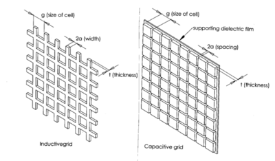
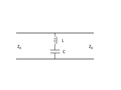
The two fundamental types of FSS are shown in Fig. 2.4.1-1 to the right - the bandpass mesh-type FSS and the bandstop patch-type FSS (Metal-mesh optical filters). The equivalent circuit for a patch-type bandstop FSS is shown in Fig. 2.4.1-2. The impedance of the series connection of the inductor and the capacitor is (Desoer, Kuh [1984]):
or,
and this series connection of an inductor and capacitor produces a zero impedance (short circuit) condition when
At the short circuit condition, all incident energy is reflected, and so this is the equivalent circuit of a resonant patch bandstop filter.
The magnitude of the reflection coefficient is:
where Z0 is the characteristic impedance of the transmission line.
The frequencies for the upper and lower 3 dB points are given as the solution to the equation:
where,
So, if the center frequency and the width of the resonance are determined from first principles codes, the L,C of the equivalent circuit may be readily obtained by fitting the reflection response of the equivalent resonant circuit to the reflection response of the actual FSS, and in this way, the circuit parameters L,C are readily extracted. Once that is done, then we can use the equivalent circuit model for multi-layer FSS design. Any nearby dielectrics should be included in the equivalent circuit.
For small values of ω, the impedance of the inductor, jωL, is smaller than the impedance of the capacitor, 1/jωC, therefore the capacitor dominates the shunt impedance and so the patch-type bandstop FSS is capacitive below resonance. We'll use this fact in section 2.3.1 to design a lowpass FSS filter using equivalent circuits.
Bandpass FSS filter equivalent circuit and transmission response
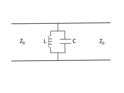
The equivalent circuit for a mesh-type bandpass FSS is shown in Fg. 2.4.2-1. The admittance of the parallel connection of inductor and capacitor is (Desoer, Kuh [1984]):
and this admittance is zero (open-circuit condition) when
When the parallel combination of inductor and capacitor produces an open circuit, all energy is transmitted.
In the same way, the magnitude of the transmission coefficient of the bandpass filter is:
Below resonance, the admittance of the inductor, 1/jωL is greater than the admittance of the capacitor jωC, therefore the mesh-type bandpass FSS is inductive below resonance.
Comparison of equivalent circuit response and actual FSS response
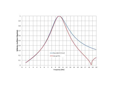
Fig. 2.4.3-1 shows the comparison in reflection between a single-layer crossed dipole FSS and its fitted equivalent circuit. The equivalent circuit is a series connection of a capacitor and inductor placed in parallel across the transmission line, as in Fig. 2.4.1-2. This resonator produces a short circuit condition at resonance. The fit is very good below the resonance though not nearly as good above.
The real FSS has a reflection null at 18.7 GHz (the frequency at which the wavelength equals the unit cell dimension of .630"), which is not accounted for in the equivalent circuit model. The null is known as a Wood's anomaly and is caused by the inverse square root singularity in the spectral domain Green's function (3.1) going to infinity. Physically, this represents a uniform plane wave propagating in the plane of the FSS. In the spatial domain, the coherent summation of all of the spatial domain Green's function's becomes infinite, so that any finite current produces an infinite field on the surface of the FSS. As a result, all currents must be zero under this condition.
This example illustrates the usefulness and shortcomings of the simple equivalent circuit model. The equivalent circuit only includes features related to the individual scattering element, not features related to the periodic array, such as interactions between the scatterers.
FSS duality versus circuit duality
FSS duality
If a mesh type FSS is created from a patch type FSS in such a way that the metal portions or the former are replaced by aperture portions of the latter, then the two FSS are said to be duals of one another. Duality only strictly applies when no dielectric substrates are present, therefore it is only approximately satisfied in practice, though even when dielectric substrates are present, duality can be useful in FSS design. As a side note, Pathological FSS patterns such as a checkerboard FSS may be treated as the limit of the patch and mesh as the patch (and aperture) size approaches the unit cell size, with electrical connections of the mesh retained in the limit. For dual FSS, the reflection coefficient of the patch will be equal to the transmission coefficient of the mesh.
Circuit duality
The dual circuit of the bandstop filter can be obtained simply equating the reflection coefficient of the bandstop FSS to the transmission coefficient of the bandpass FSS to obtain (if we use L1, C1 for the bandstop patch FSS and L2, C2 for the bandpass mesh FSS):
This produces a bandpass circuit (with parameters L2, C2) which is the dual of the bandstop circuit (with parameters L1, C1).
FSS equivalent circuits - applications to FSS design
Once the transmission line equivalent circuit has been determined, multi-layer FSS design becomes much simpler and more intuitive - like ordinary filter analysis and design. Now while it is certainly possible to design multi-layer FSS structures using first principles codes and generalized scattering matrices (GSM), it is far easier, quicker and more intuitive to use equivalent circuit models for FSS design, since it is possible to leverage decades' worth of research performed on electrical filter analysis and design and bring it to bear on FSS structures. And, FSS filters are even easier to design than waveguide filters since the incidence angle does not vary with frequency.
Butterworth lowpass filter design using FSS equivalent circuits

Starting point: prototype lumped L, C Butterworth filter
As an example of how to use FSS equivalent circuits for quick and efficient design of a practical filter, we can sketch out the process that would be followed in designing a 5-stage Butterworth filter (Hunter [2001], Matthaei [1964]) using a stack of 5 frequency selective surfaces, with 4 air spacers in between the FSS sheets.
The lowpass prototype L,C ladder network is shown in Fig. 3.1.1-1 (Hunter [2001]). The cutoff frequency will be scaled to 7 GHz and the filter will be matched to 377 Ohms (the impedance of free space) on the input and output sides. The idea we'll follow is that the shunt capacitors will eventually be replaced by sub-resonant (capacitive) patch-type FSS sheets and the series inductors will be replaced by air spacers between the 5 FSS layers. Short transmission lines are approximately equivalent to series inductors.

Transmission response of prototype lumped L, C filter
The transmission magnitude and phase response of the scaled Butterworth L,C filter is shown in Fig. 3.1.2-1. Transmission magnitude is flat in the passband (below the 7 GHz cutoff frequency) and has a monotonically decreasing skirt on the high frequency side of the passband. The phase through the filter is linear throughout the 7 GHz passband, making this filter an ideal choice for a linear phase filter application, for example in the design of an ultra-wideband filter that approximates a true time delay transmission line. This is the baseline lumped L,C filter that will be the starting point for our 5-layer FSS Butterworth filter design.
Now we begin the process of transforming the prototype Butterworth lumped L,C filter into an equivalent FSS Butterworth filter. Two modifications of the baseline lumped L,C filter will be necessary, in order to obtain the corresponding FSS filter. First, the series inductors will be replaced by their equivalent transmission line sections, and then the shunt capacitors will be replaced by capacitive frequency selective surfaces.

First transformation: replace series inductors with transmission line spacers
At this point in the development, the series inductors in the prototype L,C ladder network will now be replaced by sub-half-wavelength air spacers (which we will model as transmission lines) between the FSS layers. The thickness of the air spacers may be determined as shown in Fig. 3.1.3-1, in which we compare the ABCD matrix of a series inductor with the ABCD matrix of a short transmission line (Ramo [1994]), in order to obtain the proper length of transmission line between the shunt capacitors (sub-resonant FSS layers) to produce a Butterworth filter response. It is well known that a series inductor represents an approximate lumped circuit model of a short transmission line, and we'll exploit this equivalence to determine the required thickness of the air spacers.
With the thickness of the air spacers between sheets now determined, the equivalent circuit now takes on the form shown in Fig. 3.1.4-1:
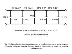
Second transformation: Replace shunt capacitors with capacitive patch FSS below resonance
Now the only thing left to do is to find the lowpass FSS that yields the shunt capacitance values called out in Fig. 2.3.1-4. This is usually done through trial and error. Fitting a shunt capacitor to a real FSS is done by repeated running of a first principles code to match the reflection response of the shunt capacitor with the reflection from a capacitive FSS. Patch-type FSS below resonance will produce a capacitive shunt admittance equivalent circuit, with closer packing of elements in the FSS sheet yielding higher shunt capacitance values in the equivalent circuit.
Examples
FSS can seemingly take on a nearly infinite number of forms, depending on the application. And now FSS are being used in the development of certain classes of meta-materials.
Classification: by form or by function
FSS are typically resonance region structures (wavelength comparable to element size and spacing). FSS can be classified either by their form or by their function. Morphologically, Munk (Munk [200]) classified FSS elements into 2 broad categories: those that are "wire-like" (one-dimensional) and those that are "patch-like" (two-dimensional) in appearance. His lifelong preference was for the one-dimensional wire-like FSS structures, and they do seem to have advantages for many applications. Frequency selective surfaces, as any type of filter, may also be classified according to their function, and these usually fall into 3 categories: low-pass, high-pass and bandpass, in addition to band-stop filters. FSS may be made to be absorptive as well, and absorption is usually over some frequency band.
Elements
A number of FSS scatterer configurations are now known, ranging from early types such as resonant dipoles, disks and squares to crossed dipoles, Jerusalem crosses, four-legged loaded slots and tripoles,
Low-pass
The FSS reflection and transmission properties are determined by both the individual scatterer and the lattice.
Band-stop or band-reject
Bandpass
Angular filters
AFA stacks
Fabrication
Typically FSSs are fabricated by chemically etching a copper-clad dielectric sheet, which may consist of Teflon (ε=2.1), Kapton, (ε=3.1), fiberglass (ε-4.5) or various forms of duroid (ε=6.0, 10.2). The sheet may range in thickness from a few thousandths of an inch to as much as 20–40 thousand.
Applications
Applications of FSS range from the mundane (microwave ovens) to the forefront of contemporary technology involving active and reconfigurable structures such as smart skins.
Microwave ovens
Antennas
Radomes EM absorbers
See also
- Fourier optics
- Bloch wave – MoM method
- Photonic crystal
- Metamaterial
- Bragg diffraction
- Diffraction grating
References
- Harrington, Roger (2001), Time-Harmonic Electromagnetic Fields, John Wiley, ISBN 978-0-471-20806-8
- Hunter, Ian, Theory and Design of Microwave Filters (IEE: 2001).
- Matthaei, George L.; Young, Leo and Jones, E. M. T., Microwave Filters, Impedance-Matching Networks, and Coupling Structures, McGraw-Hill, 1964}.
- Munk, Benedikt (2000), Frequency Selective Surfaces: Theory and Design, John Wiley, ISBN 978-0-471-37047-5
- Ramo, S.; Whinnery, J. R. and Van Duzer T., Fields and Waves in Communication Electronics, Wiley, 1994 978-0471585510}.
- Rao, S.M.; Wilton, Donald; Glisson, Allen (1982), Electromagnetic scattering by surfaces of arbitrary shape, IEEE Trans. Antennas Propagat.
- W. Mai et al., Prism-Based DGTD With a Simplified Periodic Boundary Condition to Analyze FSS With D2n Symmetry in a Rectangular Array Under Normal Incidence, in IEEE Antennas and Wireless Propagation Letters. doi: 10.1109/LAWP.2019.2902340
- Scott, Craig (1989), The Spectral Domain Method in Electromagnetics, Artech House, ISBN 0-89006-349-4
- Scott, Craig (1997), Introduction to Optics and Optical Imaging, IEEE Press, ISBN 978-0780334403, Bibcode: 1998iooi.book.....S
- Scott, Craig (1998), Analysis, Design and Testing of Integrated Structural Radomes Built Using Photonic Bandgap Structures, 1998 IEEE Aerospace Conf. Aspen CO, pp. 463 - 479, available on researchgate.net
- Scott, Craig (2002), Spectral Domain Analysis of Doped Electromagnetic Crystal Radomes Using the Method of Moments, 2002 IEEE Aerospace Conf. Big Sky MT, paper #504, pp. 2-957 - 2-963, available on researchgate.net
- Tsao, Chich-Hsing; Mittra, Raj (1982), "A Spectral Iteration Approach for Analyzing Scattering from Frequency Selective Surfaces", IEEE Transactions on Antennas and Propagation (IEEE Trans. Antennas Propagat. Vol. AP-30, No. 2, March 1982) 30 (2): 303–308, doi:10.1109/TAP.1982.1142779, Bibcode: 1982ITAP...30..303T
 |
