Engineering:Gracemont (microarchitecture)
 | |
| General Info | |
|---|---|
| Launched | November 4, 2021[1] |
| Marketed by | Intel |
| Designed by | Intel |
| Common manufacturer(s) | |
| Performance | |
| Max. CPU clock rate | 0.7 GHz to 4.3 GHz |
| Cache | |
| L1 cache | 96 KB per core:
|
| L2 cache | 2 or 4 MB per module |
| L3 cache | 3 MB per module |
| Architecture and classification | |
| Instruction set | x86-64 |
| Extensions | |
| Physical specifications | |
| Cores |
|
| Products, models, variants | |
| Product code name(s) |
|
| History | |
| Predecessor | Tremont |
| Successor | Crestmont |
Gracemont is a microarchitecture for low-power processors used in systems on a chip (SoCs) made by Intel, and is the successor to Tremont. Like its predecessor, it is also implemented as low-power cores in a hybrid design of the Alder Lake, Raptor Lake and Raptor Lake Refresh processors.[2]
Design
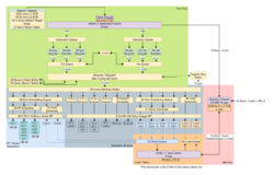
Gracemont is the fourth generation out-of-order low-power Atom microarchitecture, built on the Intel 7 manufacturing process.[3]
The Gracemont microarchitecture has the following enhancements over Tremont:[4][3]
- Level 1 cache per core:
- eight-way-associative 64 KB instruction cache
- eight-way-associative 32 KB data cache
- New On-Demand Instruction Length Decoder
- Instruction issue increased to five per clock (from four)
- Instruction retire increased to eight per clock (from seven)
- Execution ports (functional units) there are now 17 (from eight)
- Reorder buffer increased to 256 entries (from 208)
- Improved branch prediction
- Support for AVX, AVX2, FMA3 and AVX-VNNI instructions[5]
Technology
- System on a chip (SoC) architecture
- 3D tri-gate transistors
- 64 KB L1 instruction cache, up from 32 KB in Tremont[3]
- 2 or 4 MB shared L2 cache per 4-core cluster[3] Alder Lake-S/H/P/U family has 2 MB. Raptor Lake-S/H/P/U family has 4 MB.
- Intel Xe (Gen. 12.2) GPU with DirectX 12, OpenGL 4.6, Vulkan 1.3, OpenGL ES 3.2 and OpenCL 3.0 support.[6]
- Thermal design power (TDP)
- 10 W desktop processors
- 6 W mobile processors
List of Gracemont processors
The microarchitecture is used as the efficient cores of the 12th generation of Intel Core hybrid processors (codenamed "Alder Lake"), the 13th generation of Intel Core hybrid processors (codenamed "Raptor Lake") and the 14th generation of Intel Core hybrid processors (codenamed "Raptor Lake Refresh"). It's used exclusively in the Alder Lake-N line-up.
Alder Lake-N
| Branding | Model | Cores (threads) |
Clock rate (GHz) | GPU | Cache | TDP | Release date | Price (USD)[lower-alpha 1] | ||||||
|---|---|---|---|---|---|---|---|---|---|---|---|---|---|---|
| Base | Turbo | Model | EUs | Clock rate (GHz) |
L2 | L3 | Base | cTDP Down | ||||||
| Base | Turbo | |||||||||||||
| Core i3 |
N305 | 8 (8) | 1.8 | 3.8 | UHD Graphics |
32 | ? | 1.25 | 2 MB | 6 MB | 15 W | 9 W | 2023 | $309 |
| N300 | 1.1 | 7 W | N/A | |||||||||||
| Intel Processor |
N200 | 4 (4) | 1.8 | 3.7 | 0.75 | 6 W | $193 | |||||||
| N100 | 1.8 | 3.4 | 24 | $128 | ||||||||||
| N97 | 2.0 | 3.6 | 0.85 | 1.2 | 12 W | $128 | ||||||||
| N95 | 1.7 | 3.4 | 16 | ? | 15 W | ? | ||||||||
| N50 | 2 (2) | 1.0 | 3.4 | 0.6 | 0.75 | 6 W | $128 | |||||||
| Atom | x7425E | 4 (4) | 1.5 | 24 | 0.8 | 1.0 | 12 W | $58 | ||||||
| x7213E | 2 (2) | 1.7 | 3.2 | 16 | 10 W | $47 | ||||||||
| x7211E | 1.0 | 0.6 | 6 W | $39 | ||||||||||
- ↑ Price is Recommended Customer Price (RCP) at launch. RCP is the trade price that processors are sold by Intel to retailers and OEMs. Actual MSRP for consumers is higher
See also
References
- ↑ Cutress, Ian (October 27, 2021). "Intel 12th Gen Core Alder Lake for Desktops: Top SKUs Only, Coming November 4th" (in en-US). https://www.anandtech.com/show/16959/intel-innovation-alder-lake-november-4th.
- ↑ Cutress, Ian (August 14, 2020). "Intel Alder Lake: Confirmed x86 Hybrid with Golden Cove and Gracemont for 2021". https://www.anandtech.com/show/15979/intel-alder-lake-confirmed-x86-hybrid-with-golden-cove-and-gracemont-for-2021.
- ↑ 3.0 3.1 3.2 3.3 Cutress, Ian; Frumusanu, Andrei (August 19, 2021). "Intel Architecture Day 2021: Alder Lake, Golden Cove, and Gracemont Detailed" (in en-US). https://www.anandtech.com/show/16881/a-deep-dive-into-intels-alder-lake-microarchitectures.
- ↑ "Gracemont – Microarchitectures – Intel" (in en-US). https://en.wikichip.org/wiki/intel/microarchitectures/gracemont.
- ↑ Shilov, Anton (October 7, 2020). "Intel's Upcoming Gracemont Microarchitecture to Support AVX, AVX2, and AVX-VNNI". https://www.tomshardware.com/news/intels-upcoming-gracemont-microarchitecture-to-support-avx-avx2-and-avx-vnni.
- ↑ "Intel® Processor Graphics Xᵉ-LP API Developer and Optimization Guide" (in en-US). https://www.intel.com/content/www/us/en/developer/articles/guide/lp-api-developer-optimization-guide.html.
 |
