Engineering:Tensor processing unit
| Designer | |
|---|---|
| Introduced | May 2016 |
| Type | Neural network Machine learning |

A tensor processing unit (TPU) is an AI accelerator application-specific integrated circuit (ASIC) developed by Google specifically for neural network machine learning, particularly using Google's own TensorFlow software.[1] Google began using TPUs internally in 2015, and in 2018 made them available for third party use, both as part of its cloud infrastructure and by offering a smaller version of the chip for sale.
Overview
The tensor processing unit was announced in May 2016 at Google I/O, when the company said that the TPU had already been used inside their data centers for over a year.[2][3] The chip has been specifically designed for Google's TensorFlow framework, a symbolic math library which is used for machine learning applications such as neural networks.[4] However, as of 2017 Google still used CPUs and GPUs for other types of machine learning.[2] Other AI accelerator designs are appearing from other vendors also and are aimed at embedded and robotics markets.
Google's TPUs are proprietary. Some models are commercially available, and on February 12, 2018, The New York Times reported that Google "would allow other companies to buy access to those chips through its cloud-computing service."[5] Google has said that they were used in the AlphaGo versus Lee Sedol series of man-machine Go games,[3] as well as in the AlphaZero system, which produced Chess, Shogi and Go playing programs from the game rules alone and went on to beat the leading programs in those games.[6] Google has also used TPUs for Google Street View text processing and was able to find all the text in the Street View database in less than five days. In Google Photos, an individual TPU can process over 100 million photos a day. It is also used in RankBrain which Google uses to provide search results.[7]
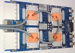
Compared to a graphics processing unit, it is designed for a high volume of low precision computation (e.g. as little as 8-bit precision)[8] with more input/output operations per joule, and lacks hardware for rasterisation/texture mapping.[3] The TPU ASICs are mounted in a heatsink assembly, which can fit in a hard drive slot within a data center rack, according to Norman Jouppi.[2]
Products
| TPUv1 | TPUv2 | TPUv3 | Edge v1 | |
|---|---|---|---|---|
| Date Introduced | 2016 | 2017 | 2018 | |
| Process Node | 28nm | 20nm? | 12nm? | |
| Die Size (mm2) | 331 | ? | ? | |
| On chip memory (MiB) | 28 | ? | ? | |
| Clock Speed (MHz) | 700 | ? | ? | |
| Memory (GB) | 8GB DDR3 | 16GB HBM | 32GB HBM | |
| TDP (W) | 40 | 200 | 250 | |
| TOPS | 23 | 45 | 90 |
First generation TPU
The first-generation TPU is an 8-bit matrix multiplication engine, driven with CISC instructions by the host processor across a PCIe 3.0 bus. It is manufactured on a 28 nm process with a die size ≤ 331 mm2. The clock speed is 700 MHz and it has a thermal design power of 28–40 W. It has 28 MiB of on chip memory, and 4 MiB of 32-bit accumulators taking the results of a 256×256 systolic array of 8-bit multipliers.[9] Within the TPU package is 8 GiB of dual-channel 2133 MHz DDR3 SDRAM offering 34 GB/s of bandwidth.[10] Instructions transfer data to or from the host, perform matrix multiplications or convolutions, and apply activation functions.[9]
Second generation TPU
The second-generation TPU was announced in May 2017.[11] Google stated the first-generation TPU design was limited by memory bandwidth and using 16 GB of High Bandwidth Memory in the second-generation design increased bandwidth to 600 GB/s and performance to 45 teraFLOPS.[10] The TPUs are then arranged into four-chip modules with a performance of 180 teraFLOPS.[11] Then 64 of these modules are assembled into 256-chip pods with 11.5 petaFLOPS of performance.[11] Notably, while the first-generation TPUs were limited to integers, the second-generation TPUs can also calculate in floating point. This makes the second-generation TPUs useful for both training and inference of machine learning models. Google has stated these second-generation TPUs will be available on the Google Compute Engine for use in TensorFlow applications.[12]
Third generation TPU
The third-generation TPU was announced on May 8, 2018.[13] Google announced that processors themselves are twice as powerful as the second-generation TPUs, and would be deployed in pods with four times as many chips as the preceding generation.[14][15] This results in an 8-fold increase in performance per pod (with up to 1,024 chips per pod) compared to the second-generation TPU deployment.
Edge TPU
In July 2018, Google announced the Edge TPU. The Edge TPU is Google's purpose-built ASIC chip designed to run machine learning (ML) models for edge computing, meaning it is much smaller and consumes far less power compared to the TPUs hosted in Google datacenters (also known as Cloud TPUs). In January 2019, Google made the Edge TPU available to developers with a line of products under the Coral brand. The Edge TPU is capable of 4 trillion operations per second while using 2W.[16]
The product offerings include a single board computer (SBC), a system on module (SoM), a USB accessory, a mini PCI-e card, and an M.2 card. The SBC Coral Dev Board and Coral SoM both run Mendel Linux OS – a derivative of Debian. The USB, PCI-e, and M.2 products function as add-ons to existing computer systems, and support Debian-based Linux systems on x86-64 and ARM64 hosts (including Raspberry Pi).
The machine learning runtime used to execute models on the Edge TPU is based on TensorFlow Lite.[17] The Edge TPU is only capable of accelerating forward-pass operations, which means it's primarily useful for performing inferences (although it is possible to perform lightweight transfer learning on the Edge TPU[18]). The Edge TPU also only supports 8-bit math, meaning that for a network to be compatible with the Edge TPU, it needs to be trained using TensorFlow quantization-aware training technique.
On November 12, 2019, Asus announced a pair of single-board computer (SBCs) featuring the Edge TPU. The Asus Tinker Edge T and Tinker Edge R Board designed for IoT and edge AI. The SBCs support Android and Debian operating systems.[19][20] ASUS has also demonstrated a mini PC called Asus PN60T featuring the Edge TPU.[21]
On January 2, 2020, Google announced the Coral Accelerator Module and Coral Dev Board Mini, to be demonstrated at CES 2020 later the same month. The Coral Accelerator Module is a multi-chip module featuring the Edge TPU, PCIe and USB interfaces for easier integration. The Coral Dev Board Mini is a smaller SBC featuring the Coral Accelerator Module and MediaTek 8167s SoC.[22][23]
Pixel Neural Core
On October 15, 2019, Google announced the Pixel 4 featuring the Pixel Neural Core, which contains an instantiation of the Edge TPU architecture.[24]
See also
- Vision processing unit a similar device specialised for vision processing.
- TrueNorth a similar device simulating spiking neurons instead of low precision tensors.
- Neural processing unit
- Cognitive computer
- Tensor Core, a similar architecture proposed by Nvidia
References
- ↑ "Cloud Tensor Processing Units (TPUs)". https://cloud.google.com/tpu/docs/tpus. Retrieved 20 July 2020.
- ↑ 2.0 2.1 2.2 "Google's Tensor Processing Unit explained: this is what the future of computing looks like" (in en). TechRadar. http://www.techradar.com/news/computing-components/processors/google-s-tensor-processing-unit-explained-this-is-what-the-future-of-computing-looks-like-1326915.
- ↑ 3.0 3.1 3.2 Jouppi, Norm (May 18, 2016). "Google supercharges machine learning tasks with TPU custom chip" (in en-US). https://cloudplatform.googleblog.com/2016/05/Google-supercharges-machine-learning-tasks-with-custom-chip.html.
- ↑ "TensorFlow: Open source machine learning" "It is machine learning software being used for various kinds of perceptual and language understanding tasks" — Jeffrey Dean, minute 0:47 / 2:17 from Youtube clip
- ↑ "Google Makes Its Special A.I. Chips Available to Others" (in en). The New York Times. https://www.nytimes.com/2018/02/12/technology/google-artificial-intelligence-chips.html.
- ↑ McGourty, Colin (6 December 2017). "DeepMind's AlphaZero crushes chess" (in en). https://chess24.com/en/read/news/deepmind-s-alphazero-crushes-chess.
- ↑ "Google's Tensor Processing Unit could advance Moore's Law 7 years into the future" (in en). PCWorld. http://www.pcworld.com/article/3072256/google-io/googles-tensor-processing-unit-said-to-advance-moores-law-seven-years-into-the-future.html.
- ↑ Armasu, Lucian (2016-05-19). "Google's Big Chip Unveil For Machine Learning: Tensor Processing Unit With 10x Better Efficiency (Updated)". http://www.tomshardware.com/news/google-tensor-processing-unit-machine-learning,31834.html.
- ↑ 9.0 9.1 Jouppi, Norman P.; Young, Cliff; Patil, Nishant; Patterson, David; Agrawal, Gaurav; Bajwa, Raminder; Bates, Sarah; Bhatia, Suresh et al. (June 26, 2017). "In-Datacenter Performance Analysis of a Tensor Processing Unit™". Toronto, Canada.
- ↑ 10.0 10.1 Kennedy, Patrick (22 August 2017). "Case Study on the Google TPU and GDDR5 from Hot Chips 29". Serve The Home. https://www.servethehome.com/case-study-google-tpu-gddr5-hot-chips-29/. Retrieved 23 August 2017.
- ↑ 11.0 11.1 11.2 Bright, Peter (17 May 2017). "Google brings 45 teraflops tensor flow processors to its compute cloud". Ars Technica. https://arstechnica.com/information-technology/2017/05/google-brings-45-teraflops-tensor-flow-processors-to-its-compute-cloud/. Retrieved 30 May 2017.
- ↑ Kennedy, Patrick (17 May 2017). "Google Cloud TPU Details Revealed". Serve The Home. https://www.servethehome.com/google-cloud-tpu-details-revealed/. Retrieved 30 May 2017.
- ↑ Frumusanu, Andre (8 May 2018). "Google I/O Opening Keynote Live-Blog". https://www.anandtech.com/show/12726/google-io-keynote-liveblog-10am-pt. Retrieved 9 May 2018.
- ↑ Feldman, Michael (11 May 2018). "Google Offers Glimpse of Third-Generation TPU Processor". Top 500. https://www.top500.org/news/google-offers-glimpse-of-third-generation-tpu-processor/. Retrieved 14 May 2018.
- ↑ Teich, Paul (10 May 2018). "Tearing Apart Google's TPU 3.0 AI Coprocessor". The Next Platform. https://www.nextplatform.com/2018/05/10/tearing-apart-googles-tpu-3-0-ai-coprocessor/. Retrieved 14 May 2018.
- ↑ "Edge TPU performance benchmarks" (in en-us). https://coral.ai/docs/edgetpu/benchmarks/.
- ↑ "Bringing intelligence to the edge with Cloud IoT" (in en-US). 2018-07-25. https://www.blog.google/products/google-cloud/bringing-intelligence-to-the-edge-with-cloud-iot/.
- ↑ "Retrain an image classification model on-device". https://coral.withgoogle.com/docs/edgetpu/retrain-classification-ondevice/.
- ↑ "組込み総合技術展&IoT総合技術展「ET & IoT Technology 2019」に出展することを発表" (in ja-JP). https://www.asus.com/jp/News/jr4skqts65jsuggg.
- ↑ Shilov, Anton. "ASUS & Google Team Up for 'Tinker Board' AI-Focused Credit-Card Sized Computers". https://www.anandtech.com/show/15095/asus-google-team-up-for-tinker-board-aifocused-creditcard-sized-computers.
- ↑ Aufranc, Jean-Luc (2019-05-29). "ASUS Tinker Edge T & CR1S-CM-A SBC to Feature Google Coral Edge TPU & NXP i.MX 8M Processor" (in en-US). https://www.cnx-software.com/2019/05/29/asus-tinker-edge-t-cr1s-cm-a-sbc-google-coral-edge-tpu-nxp-i-mx-8m-processor.
- ↑ "New Coral products for 2020" (in en). https://developers.googleblog.com/2020/01/new-coral-products-for-2020.html.
- ↑ "Accelerator Module" (in en-us). https://coral.ai/products/accelerator-module.
- ↑ "Introducing the Next Generation of On-Device Vision Models: MobileNetV3 and MobileNetEdgeTPU" (in en). http://ai.googleblog.com/2019/11/introducing-next-generation-on-device.html.
External links
- Cloud Tensor Processing Units (TPUs) (Documentation from Google Cloud)
- Photo of Google's TPU chip and board
- Photo of Google's TPU v2 board
- Photo of Google's TPU v3 board
- Photo of Google's TPU v2 pod

