Engineering:Application-specific integrated circuit
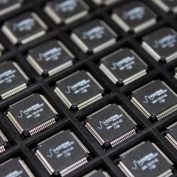
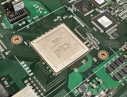
An application-specific integrated circuit (ASIC /ˈeɪsɪk/) is an integrated circuit (IC) chip customized for a particular use, rather than intended for general-purpose use, such as a chip designed to run in a digital voice recorder or a high-efficiency video codec. Application-specific standard product chips are intermediate between ASICs and industry standard integrated circuits like the 7400 series or the 4000 series.[1] ASIC chips are typically fabricated using metal–oxide–semiconductor (MOS) technology, as MOS integrated circuit chips.[2]
As feature sizes have shrunk and chip design tools improved over the years, the maximum complexity (and hence functionality) possible in an ASIC has grown from 5,000 logic gates to over 100 million. Modern ASICs often include entire microprocessors, memory blocks including ROM, RAM, EEPROM, flash memory and other large building blocks. Such an ASIC is often termed a SoC (system-on-chip). Designers of digital ASICs often use a hardware description language (HDL), such as Verilog or VHDL, to describe the functionality of ASICs.[1]
Field-programmable gate arrays (FPGA) are the modern-day technology improvement on breadboards, meaning that they are not made to be application-specific as opposed to ASICs. Programmable logic blocks and programmable interconnects allow the same FPGA to be used in many different applications. For smaller designs or lower production volumes, FPGAs may be more cost-effective than an ASIC design, even in production. The non-recurring engineering (NRE) cost of an ASIC can run into the millions of dollars. Therefore, device manufacturers typically prefer FPGAs for prototyping and devices with low production volume and ASICs for very large production volumes where NRE costs can be amortized across many devices.[3]
History
Early ASICs used gate array technology. By 1967, Ferranti and Interdesign were manufacturing early bipolar gate arrays. In 1967, Fairchild Semiconductor introduced the Micromatrix family of bipolar diode–transistor logic (DTL) and transistor–transistor logic (TTL) arrays.[2]
Complementary metal–oxide–semiconductor (CMOS) technology opened the door to the broad commercialization of gate arrays. The first CMOS gate arrays were developed by Robert Lipp,[4][5] in 1974 for International Microcircuits, Inc. (IMI).[2]
Metal–oxide–semiconductor (MOS) standard-cell technology was introduced by Fairchild and Motorola, under the trade names Micromosaic and Polycell, in the 1970s. This technology was later successfully commercialized by VLSI Technology (founded 1979) and LSI Logic (1981).[2]
A successful commercial application of gate array circuitry was found in the low-end 8-bit ZX81 and ZX Spectrum personal computers, introduced in 1981 and 1982. These were used by Sinclair Research (UK) essentially as a low-cost I/O solution aimed at handling the computer's graphics.
Customization occurred by varying a metal interconnect mask. Gate arrays had complexities of up to a few thousand gates; this is now called mid-scale integration. Later versions became more generalized, with different base dies customized by both metal and polysilicon layers. Some base dies also include random-access memory (RAM) elements.
Standard-cell designs
In the mid-1980s, a designer would choose an ASIC manufacturer and implement their design using the design tools available from the manufacturer. While third-party design tools were available, there was not an effective link from the third-party design tools to the layout and actual semiconductor process performance characteristics of the various ASIC manufacturers. Most designers used factory-specific tools to complete the implementation of their designs. A solution to this problem, which also yielded a much higher density device, was the implementation of standard cells.[6] Every ASIC manufacturer could create functional blocks with known electrical characteristics, such as propagation delay, capacitance and inductance, that could also be represented in third-party tools. Standard-cell design is the utilization of these functional blocks to achieve very high gate density and good electrical performance. Standard-cell design is intermediate between § Gate-array and semi-custom design and § Full-custom design in terms of its non-recurring engineering and recurring component costs as well as performance and speed of development (including time to market).
By the late 1990s, logic synthesis tools became available. Such tools could compile HDL descriptions into a gate-level netlist. Standard-cell integrated circuits (ICs) are designed in the following conceptual stages referred to as electronics design flow, although these stages overlap significantly in practice:
- Requirements engineering: A team of design engineers starts with a non-formal understanding of the required functions for a new ASIC, usually derived from requirements analysis.
- Register-transfer level (RTL) design: The design team constructs a description of an ASIC to achieve these goals using a hardware description language. This process is similar to writing a computer program in a high-level language.
- Functional verification: Suitability for purpose is verified by functional verification. This may include such techniques as logic simulation through test benches, formal verification, emulation, or creating and evaluating an equivalent pure software model, as in Simics. Each verification technique has advantages and disadvantages, and most often several methods are used together for ASIC verification. Unlike most FPGAs, ASICs cannot be reprogrammed once fabricated and therefore ASIC designs that are not completely correct are much more costly, increasing the need for full test coverage.
- Logic synthesis: Logic synthesis transforms the RTL design into a large collection called of lower-level constructs called standard cells. These constructs are taken from a standard-cell library consisting of pre-characterized collections of logic gates performing specific functions. The standard cells are typically specific to the planned manufacturer of the ASIC. The resulting collection of standard cells and the needed electrical connections between them is called a gate-level netlist.
- Placement: The gate-level netlist is next processed by a placement tool which places the standard cells onto a region of an integrated circuit die representing the final ASIC. The placement tool attempts to find an optimized placement of the standard cells, subject to a variety of specified constraints.
- Routing: An electronics routing tool takes the physical placement of the standard cells and uses the netlist to create the electrical connections between them. Since the search space is large, this process will produce a "sufficient" rather than "globally optimal" solution. The output is a file which can be used to create a set of photomasks enabling a semiconductor fabrication facility, commonly called a 'fab' or 'foundry' to manufacture physical integrated circuits. Placement and routing are closely interrelated and are collectively called place and route in electronics design.
- Sign-off: Given the final layout, circuit extraction computes the parasitic resistances and capacitances. In the case of a digital circuit, this will then be further mapped into delay information from which the circuit performance can be estimated, usually by static timing analysis. This, and other final tests such as design rule checking and power analysis collectively called signoff are intended to ensure that the device will function correctly over all extremes of the process, voltage and temperature. When this testing is complete the photomask information is released for chip fabrication.
These steps, implemented with a level of skill common in the industry, almost always produce a final device that correctly implements the original design, unless flaws are later introduced by the physical fabrication process.[7]
The design steps also called design flow, are also common to standard product design. The significant difference is that standard-cell design uses the manufacturer's cell libraries that have been used in potentially hundreds of other design implementations and therefore are of much lower risk than a full custom design. Standard cells produce a design density that is cost-effective, and they can also integrate IP cores and static random-access memory (SRAM) effectively, unlike gate arrays.
Gate-array and semi-custom design
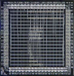
Gate array design is a manufacturing method in which diffused layers, each consisting of transistors and other active devices, are predefined and electronics wafers containing such devices are "held in stock" or unconnected prior to the metallization stage of the fabrication process. The physical design process defines the interconnections of these layers for the final device. For most ASIC manufacturers, this consists of between two and nine metal layers with each layer running perpendicular to the one below it. Non-recurring engineering costs are much lower than full custom designs, as photolithographic masks are required only for the metal layers. Production cycles are much shorter, as metallization is a comparatively quick process; thereby accelerating time to market.
Gate-array ASICs are always a compromise between rapid design and performance as mapping a given design onto what a manufacturer held as a stock wafer never gives 100% circuit utilization. Often difficulties in routing the interconnect require migration onto a larger array device with a consequent increase in the piece part price. These difficulties are often a result of the layout EDA software used to develop the interconnect.
Pure, logic-only gate-array design is rarely implemented by circuit designers today, having been almost entirely replaced by field-programmable devices. The most prominent of such devices are field-programmable gate arrays (FPGAs) which can be programmed by the user and thus offer minimal tooling charges, non-recurring engineering, only marginally increased piece part cost, and comparable performance.
Today, gate arrays are evolving into structured ASICs that consist of a large IP core like a CPU, digital signal processor units, peripherals, standard interfaces, integrated memories, SRAM, and a block of reconfigurable, uncommitted logic. This shift is largely because ASIC devices are capable of integrating large blocks of system functionality, and systems on a chip (SoCs) require glue logic, communications subsystems (such as networks on chip), peripherals, and other components rather than only functional units and basic interconnection.
In their frequent usages in the field, the terms "gate array" and "semi-custom" are synonymous when referring to ASICs. Process engineers more commonly use the term "semi-custom", while "gate-array" is more commonly used by logic (or gate-level) designers.
Full-custom design
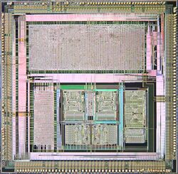
By contrast, full-custom ASIC design defines all the photolithographic layers of the device.[6] Full-custom design is used for both ASIC design and for standard product design.
The benefits of full-custom design include reduced area (and therefore recurring component cost), performance improvements, and also the ability to integrate analog components and other pre-designed—and thus fully verified—components, such as microprocessor cores, that form a system on a chip.
The disadvantages of full-custom design can include increased manufacturing and design time, increased non-recurring engineering costs, more complexity in the computer-aided design (CAD) and electronic design automation systems, and a much higher skill requirement on the part of the design team.
For digital-only designs, however, "standard-cell" cell libraries, together with modern CAD systems, can offer considerable performance/cost benefits with low risk. Automated layout tools are quick and easy to use and also offer the possibility to "hand-tweak" or manually optimize any performance-limiting aspect of the design.
This is designed by using basic logic gates, circuits or layout specially for a design.
Structured design
Structured ASIC design (also referred to as "platform ASIC design") is a relatively new trend in the semiconductor industry, resulting in some variation in its definition. However, the basic premise of a structured ASIC is that both manufacturing cycle time and design cycle time are reduced compared to cell-based ASIC, by virtue of there being pre-defined metal layers (thus reducing manufacturing time) and pre-characterization of what is on the silicon (thus reducing design cycle time).
Definition from Foundations of Embedded Systems states that:[8]
In a "structured ASIC" design, the logic mask-layers of a device are predefined by the ASIC vendor (or in some cases by a third party). Design differentiation and customization is achieved by creating custom metal layers that create custom connections between predefined lower-layer logic elements. "Structured ASIC" technology is seen as bridging the gap between field-programmable gate arrays and "standard-cell" ASIC designs. Because only a small number of chip layers must be custom-produced, "structured ASIC" designs have much smaller non-recurring expenditures (NRE) than "standard-cell" or "full-custom" chips, which require that a full mask set be produced for every design.
This is effectively the same definition as a gate array. What distinguishes a structured ASIC from a gate array is that in a gate array, the predefined metal layers serve to make manufacturing turnaround faster. In a structured ASIC, the use of predefined metallization is primarily to reduce cost of the mask sets as well as making the design cycle time significantly shorter.
For example, in a cell-based or gate-array design the user must often design power, clock, and test structures themselves. By contrast, these are predefined in most structured ASICs and therefore can save time and expense for the designer compared to gate-array based designs. Likewise, the design tools used for structured ASIC can be substantially lower cost and easier (faster) to use than cell-based tools, because they do not have to perform all the functions that cell-based tools do. In some cases, the structured ASIC vendor requires customized tools for their device (e.g., custom physical synthesis) be used, also allowing for the design to be brought into manufacturing more quickly.
Cell libraries, IP-based design, hard and soft macros
Cell libraries of logical primitives are usually provided by the device manufacturer as part of the service. Although they will incur no additional cost, their release will be covered by the terms of a non-disclosure agreement (NDA) and they will be regarded as intellectual property by the manufacturer. Usually, their physical design will be pre-defined so they could be termed "hard macros".
What most engineers understand as "intellectual property" are IP cores, designs purchased from a third-party as sub-components of a larger ASIC. They may be provided in the form of a hardware description language (often termed a "soft macro"), or as a fully routed design that could be printed directly onto an ASIC's mask (often termed a "hard macro"). Many organizations now sell such pre-designed cores – CPUs, Ethernet, USB or telephone interfaces – and larger organizations may have an entire department or division to produce cores for the rest of the organization. The company ARM only sells IP cores, making it a fabless manufacturer.
Indeed, the wide range of functions now available in structured ASIC design is a result of the phenomenal improvement in electronics in the late 1990s and early 2000s; as a core takes a lot of time and investment to create, its re-use and further development cuts product cycle times dramatically and creates better products. Additionally, open-source hardware organizations such as OpenCores are collecting free IP cores, paralleling the open-source software movement in hardware design.
Soft macros are often process-independent (i.e. they can be fabricated on a wide range of manufacturing processes and different manufacturers). Hard macros are process-limited and usually further design effort must be invested to migrate (port) to a different process or manufacturer.
Multi-project wafers
Some manufacturers and IC design houses offer multi-project wafer service (MPW) as a method of obtaining low cost prototypes. Often called shuttles, these MPWs, containing several designs, run at regular, scheduled intervals on a "cut and go" basis, usually with limited liability on the part of the manufacturer. The contract involves delivery of bare dies or the assembly and packaging of a handful of devices. The service usually involves the supply of a physical design database (i.e. masking information or pattern generation (PG) tape). The manufacturer is often referred to as a "silicon foundry" due to the low involvement it has in the process.
Application-specific standard product
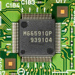
An application-specific standard product or ASSP is an integrated circuit that implements a specific function that appeals to a wide market. As opposed to ASICs that combine a collection of functions and are designed by or for one customer, ASSPs are available as off-the-shelf components. ASSPs are used in all industries, from automotive to communications.[citation needed] As a general rule, if you can find a design in a data book, then it is probably not an ASIC, but there are some exceptions.[clarification needed]
For example, two ICs that might or might not be considered ASICs are a controller chip for a PC and a chip for a modem. Both of these examples are specific to an application (which is typical of an ASIC) but are sold to many different system vendors (which is typical of standard parts). ASICs such as these are sometimes called application-specific standard products (ASSPs).
Examples of ASSPs are encoding/decoding chip, Ethernet network interface controller chip, etc.
See also
- Application-specific instruction set processor (ASIP)
- Complex programmable logic device (CPLD)
- Electronic design automation (EDA or ECAD)
- Field-programmable gate array (FPGA)
- Multi-project chip (MPC)
- Very Large Scale Integration (VLSI)
- System on a chip (SoC)
- Hardware acceleration for an overview of computing based primarily in hardware
References
- ↑ 1.0 1.1 Barr, Keith (2007). ASIC Design in the Silicon Sandbox: A Complete Guide to Building Mixed-signal Integrated Circuits. New York: McGraw-Hill. ISBN 978-0-07-148161-8. OCLC 76935560. https://archive.org/details/asicdesigninsili0000barr.
- ↑ 2.0 2.1 2.2 2.3 "1967: Application Specific Integrated Circuits employ Computer-Aided Design". Computer History Museum. https://www.computerhistory.org/siliconengine/application-specific-integrated-circuits-employ-computer-aided-design/.
- ↑ Kriegbaum, Jeff (13 September 2004). "FPGA's vs. ASIC's". https://www.eetimes.com/fpgas-vs-asics/.
- ↑ Lipp, Bob oral history. Computer History Museum. 14 February 2017. http://www.computerhistory.org/collections/catalog/102706880. Retrieved 2018-01-28.
- ↑ "People". Computer History Museum. http://www.computerhistory.org/siliconengine/people/.
- ↑ 6.0 6.1 Smith, Michael John Sebastian (1997). Application-Specific Integrated Circuits. Addison-Wesley Professional. ISBN 978-0-201-50022-6.
- ↑ Hurley, Jaden Mclean & Carmen. (2019). Logic Design. EDTECH. ISBN 978-1-83947-319-7. OCLC 1132366891.
- ↑ Barkalov, Alexander; Titarenko, Larysa; Mazurkiewicz, Małgorzata (2019) (in en). Foundations of Embedded Systems. Studies in Systems, Decision and Control. 195. Cham: Springer International Publishing. doi:10.1007/978-3-030-11961-4. ISBN 9783030119607.
Sources
- Barr, Keith (2007). ASIC Design in the Silicon Sandbox: A Complete Guide to Building Mixed-Signal Integrated Circuits. McGraw Hill Professional. ISBN 978-0-07-148161-8.
- Anthony Cataldo (26 March 2002). "Xilinx looks to ease path to custom FPGAs". EE Times (CMP Media, LLC). http://www.eetimes.com/story/OEG20020325S0060.
- "Xilinx intros next-gen EasyPath FPGAs priced below structured ASICs". EDP Weekly's IT Monitor (Millin Publishing, Inc.). 18 October 2004. http://www.thefreelibrary.com/Xilinx+intros+next-gen+EasyPath+FPGAs+priced+below+structured+ASICs.-a0125948398.
- Golshan, K. (2007). Physical design essentials: an ASIC design implementation perspective. New York: Springer. ISBN 978-0-387-36642-5.
External links
 |
