Chemistry:Gallium indium antimonide
Gallium indium antimonide, also known as indium gallium antimonide, GaInSb, or InGaSb (GaxIn1-xSb), is a ternary III-V semiconductor compound. It can be considered as an alloy between gallium antimonide and indium antimonide. The alloy can contain any ratio between gallium and indium. GaInSb refers generally to any composition of the alloy.
Preparation
GaInSb films have been grown by molecular beam epitaxy[1], chemical beam epitaxy[2] and liquid phase epitaxy[3] on gallium arsenide and gallium antimonide substrates. It is often incorporated into layered heterostructures with other III-V compounds.
Electronic Properties

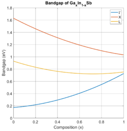
The bandgap and lattice constant of GaInSb alloys are between those of pure GaSb (a = 0.610 nm, Eg = 0.73 eV) and InSb (a = 0.648 nm, Eg = 0.17 eV).[4] Over all compositions, the bandgap is direct, like in pure GaSb and InSb.
Applications
InGaSb and InGaSb-containing heterostructures have been studied for use in near- to mid-infrared photodetectors,[6][7][8] transistors,[9][10] and hall effect sensors.[11]
References
- ↑ "Molecular beam epitaxy of GaSb and InGaSb". Journal of Crystal Growth 73 (3): 641–645. 1985. doi:10.1016/0022-0248(85)90031-4.
- ↑ "MOMBE (Metalorganic Molecular Beam Epitaxy) growth of InGaSb on GaSb". Journal of Crystal Growth 95 (1): 158–162. 1989. doi:10.1016/0022-0248(89)90372-2.
- ↑ "Solution growth of thick III–V antimonide alloy epilayers (InAsSb, InGaSb, InGaAsSb, AlGaAsSb, and InAsSbP) for "virtual substrates"". Journal of Crystal Growth 225 (2): 236–243. 2001. doi:10.1016/S0022-0248(01)00843-0.
- ↑ 4.0 4.1 "Band parameters for III–V compound semiconductors and their alloys". Journal of Applied Physics 89 (11): 5815–5875. 2001. doi:10.1063/1.1368156. Bibcode: 2001JAP....89.5815V.
- ↑ "Band gaps and refractive indices of AlGaAsSb, GaInAsSb, and InPAsSb: Key properties for a variety of the 2–4 μm optoelectronic device applications". Journal of Applied Physics 61 (10): 4869–4876. 1987. doi:10.1063/1.338352.
- ↑ "InAs/GaInSb superlattices as a promising material system for third generation infrared detectors". Infrared Physics & Technology 48 (1): 39–52. 2006. doi:10.1016/j.infrared.2005.01.003.
- ↑ "Ultra-fast photodetectors based on high-mobility indium gallium antimonide nanowires". Nature Communications (Nature Publishing Group) 10 (1): 1664. 2019. doi:10.1038/s41467-019-09606-y. PMID 30971702.
- ↑ "InGaSb photodetectors using an InGaSb substrate for 2μm applications". Applied Physics Letters 85 (11): 1874–1876. 2004. doi:10.1063/1.1787893.
- ↑ "Device Characteristics of InGaSb/AlSb High-Hole-Mobility FETs". IEEE Electron Device Letters 33 (7): 964–966. 2012. doi:10.1109/LED.2012.2193656.
- ↑ "Molecular beam epitaxial growth of metamorphic AlInSb/GaInSb high-electron-mobility-transistor structures on GaAs substrates for low power and high frequency applications". Journal of Applied Physics 109 (3): 033706. 2011. doi:10.1063/1.3544041.
- ↑ "Temperature stable Hall effect sensors". IEEE Sensors Journal 6 (1): 106–110. 2006. doi:10.1109/JSEN.2005.860362.
External links
 |

