Chemistry:Gallium(II) selenide

| |

| |
| Names | |
|---|---|
| IUPAC name
Gallium selenide
| |
| Other names
Gallium monoselenide
| |
| Identifiers | |
3D model (JSmol)
|
|
| ChemSpider | |
PubChem CID
|
|
| |
| |
| Properties | |
| GaSe | |
| Molar mass | 148.69 g/mol |
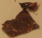
| Appearance | brown solid |
| Density | 5.03 g/cm3 |
| Melting point | 960 °C (1,760 °F; 1,230 K) |
| Band gap | 2.1 eV (indirect) |
Refractive index (nD)
|
2.6 |
| Structure | |
| hexagonal, hP8 | |
| P63/mmc, No. 194 | |
| Related compounds | |
Other anions
|
Gallium(II) oxide, Gallium(II) sulfide, Gallium(II) telluride |
Other cations
|
Zinc(II) selenide, Germanium monoselenide, Indium monoselenide |
Related compounds
|
Gallium(III) selenide |
Except where otherwise noted, data are given for materials in their standard state (at 25 °C [77 °F], 100 kPa). | |
| Infobox references | |
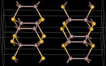
Gallium(II) selenide (GaSe) is a chemical compound. It has a hexagonal layer structure, similar to that of GaS.[1] It is a photoconductor,[2] a second harmonic generation crystal in nonlinear optics,[3] and has been used as a far-infrared conversion material[4] at 14–31 THz and above.[5]
Uses
It is said to have potential for optical applications[6] but the exploitation of this potential has been limited by the ability to readily grow single crystals[7] Gallium selenide crystals show great promise as a nonlinear optical material and as a photoconductor. Non-linear optical materials are used in the frequency conversion of laser light. Frequency conversion involves the shifting of the wavelength of a monochromatic source of light, usually laser light, to a higher or lower wavelength of light that cannot be produced from a conventional laser source.
Several methods of frequency conversion using non-linear optical materials exist. Second harmonic generation leads to doubling of the frequency of infrared carbon dioxide lasers. In optical parametric generation, the wavelength of light is doubled. Near-infrared solid-state lasers are usually used in optical parametric generations.[8]
One original problem with using gallium selenide in optics is that it is easily broken along cleavage lines and thus it can be hard to cut for practical application. It has been found, however, that doping the crystals with indium greatly enhances their structural strength and makes their application much more practical.[7] There remain, however, difficulties with crystal growth that must be overcome before gallium selenide crystals may become more widely used in optics.
Single layers of gallium selenide are dynamically stable two-dimensional semiconductors, in which the valence band has an inverted Mexican-hat shape, leading to a Lifshitz transition as the hole-doping is increased.[9]
The integration of gallium selenide into electronic devices has been hindered by its air sensitivity. Several approaches have been developed to encapsulate GaSe mono- and few-layers, leading to improved chemical stability and electronic mobility.[10][11][12]
Synthesis
Synthesis of GaSe nanoparticles is carried out by the reaction of GaMe3 with trioctylphosphine selenium (TOPSe) in a high temperature solution of trioctylphosphine (TOP) and trioctylphosphine oxide (TOPO).[13]
- GaMe3 + P[(CH2)7CH3]3Se → GaSe
A solution of 15 g TOPO and 5 mL TOP is heated to 150 °C overnight under nitrogen, removing any water that may be present in the original TOP solution. This initial TOP solution is vacuum distilled at 0.75 torr, taking the fraction from 204 °C to 235 °C. A TOPSe solution (12.5 mL TOP with 1.579 g TOPSe) is then added and the TOPO/TOP/TOPSe reaction mixture is heated to 278 °C. GaMe3 (0.8 mL) dissolved in 7.5 mL distilled TOP is then injected. After injection, the temperature drops to 254 °C before stabilizing in the range of 266–268 °C after 10 minutes. GaSe nanoparticles then begin to form, and may be detected by a shoulder in the optical absorption spectrum in the 400–450 nm range. After this shoulder is observed, the reaction mixture is left to cool to room temperature to prevent further reaction. After synthesis and cooling, the reaction vessel is opened and extraction of the GaSe nanoparticle solution is accomplished by addition of methanol. The distribution of nanoparticles between the polar (methanol) and non-polar (TOP) phases depends on experimental conditions. If the mixture is very dry, nanoparticles partition into the methanol phase. If the nanoparticles are exposed to air or water, however, the particles become uncharged and become partitioned into the non-polar TOP phase.[13]
References
- ↑ Greenwood, Norman N.; Earnshaw, Alan (1997). Chemistry of the Elements (2nd ed.). Butterworth-Heinemann. ISBN 978-0-08-037941-8.
- ↑ Richard H. Bube; Edward L. Lind (1959). "Photoconductivity of Gallium Selenide Crystals". Phys. Rev. 115 (5): 1159–1164. doi:10.1103/PhysRev.115.1159. Bibcode: 1959PhRv..115.1159B.
- ↑ J. M. Auerhammer; E. R. Eliel (1996). "Frequency doubling of mid-infrared radiation in gallium selenide". Opt. Lett. 21 (11): 773–775. doi:10.1364/OL.21.000773. PMID 19876154. Bibcode: 1996OptL...21..773A.
- ↑ N.B. Singh; D.R. Suhre; V. Balakrishna; M. Marable*; R. Meyer*; N. Fernelius; F.K. Hopkins; D. Zelmon (1998). "Far-infrared conversion materials: Gallium selenide for far-infrared conversion applications". Progress in Crystal Growth and Characterization of Materials 37 (1): 47–102. doi:10.1016/S0960-8974(98)00013-8.
- ↑ Kübler, C. (2005). Kobayashi, Takayoshi; Okada, Tadashi; Kobayashi, Tetsuro et al.. eds. Ultrabroadband detection of multi-THz field transients with GaSe electro-optic sensors. Springer Series in Chemical Physics. 79. doi:10.1007/b138761. ISBN 3-540-24110-8. https://cds.cern.ch/record/1339314/files/978-3-540-27213-7_BookTOC.pdf.
- ↑ Liska, P.; Thampi, K.; Gratzel, M.; Bremaud, D.; Rudmann, D.; Upadhyaya, H. (2006). "Nanocrystalline dye-sensitized solar cell/copper indium gallium selenide thin-film tandem showing greater than 15% conversion efficiency". Applied Physics Letters 88 (20): 203103. doi:10.1063/1.2203965. Bibcode: 2006ApPhL..88t3103L.
- ↑ 7.0 7.1 V. G. Voevodin (2004). "Large single crystals of gallium selenide: growing, doping by In and characterization". Optical Materials 26 (4): 495–499. doi:10.1016/j.optmat.2003.09.014. Bibcode: 2004OptMa..26..495V.
- ↑ B. Singh (1998). "Far-infrared conversion materials: Gallium selenide for far-infrared conversion applications". Progress in Crystal Growth and Characterization of Materials 37: 47. doi:10.1016/S0960-8974(98)00013-8.
- ↑ V. Zolyomi; N. D. Drummond; V. I. Fal'ko (2013). "Band structure and optical transitions in atomic layers of hexagonal gallium chalcogenides". Phys. Rev. B 87 (19): 195403. doi:10.1103/PhysRevB.87.195403. Bibcode: 2013PhRvB..87s5403Z.
- ↑ Arora, Himani; Jung, Younghun; Venanzi, Tommaso; Watanabe, Kenji; Taniguchi, Takashi; Hübner, René; Schneider, Harald; Helm, Manfred et al. (2019-11-20). "Effective Hexagonal Boron Nitride Passivation of Few-Layered InSe and GaSe to Enhance Their Electronic and Optical Properties". ACS Applied Materials & Interfaces 11 (46): 43480–43487. doi:10.1021/acsami.9b13442. ISSN 1944-8244. PMID 31651146. https://doi.org/10.1021/acsami.9b13442.
- ↑ Arora, Himani; Erbe, Artur (2021). "Recent progress in contact, mobility, and encapsulation engineering of InSe and GaSe" (in en). InfoMat 3 (6): 662–693. doi:10.1002/inf2.12160. ISSN 2567-3165.
- ↑ Arora, Himani (2020). "Charge transport in two-dimensional materials and their electronic applications". https://himani-arora-ha.github.io/pdf/Dissertation.pdf.
- ↑ 13.0 13.1 Chikan, V.; Kelley, D. (2002). "Synthesis of Highly Luminescent Nanoparticles". Nano Letters 2 (2): 141. doi:10.1021/nl015641m. Bibcode: 2002NanoL...2..141C.
External links
- Gallium Selenide Nanoparticles Used In Solar Energy Conversion (ScienceDaily).
 |
