Biography:Leo Esaki
Leo Esaki | |
|---|---|
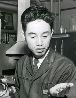
 Esaki in 1959 | |
| Born | March 12, 1925[1] Takaida-mura, Nakakawachi-gun, Osaka Prefecture, Empire of Japan |
| Alma mater | Tokyo Imperial University |
| Known for |
|
| Spouse(s) |
|
| Children | 3 |
| Awards |
|
| Scientific career | |
| Fields | |
| Institutions |
|
Reona Esaki (江崎 玲於奈 Esaki Reona, born March 12, 1925), also known as Leo Esaki, is a Japanese physicist who shared the Nobel Prize in Physics in 1973 with Ivar Giaever and Brian David Josephson for his work in electron tunneling in semiconductor materials which finally led to his invention of the Esaki diode, which exploited that phenomenon. This research was done when he was with Tokyo Tsushin Kogyo (now known as Sony). He has also contributed in being a pioneer of the semiconductor superlattices.[1]
Early life and education
Esaki was born in Takaida-mura, Nakakawachi-gun, Osaka Prefecture (now part of Higashiōsaka City) and grew up in Kyoto, near by Kyoto Imperial University and Doshisha University. He first had contact with American culture in Doshisha Junior High School (ja). After graduating from the Third Higher School, he studied physics at Tokyo Imperial University, where he had attended Hideki Yukawa's course in nuclear theory in October 1944. Also, he lived through the Bombing of Tokyo while he was at college.[2]
Esaki received his B.Sc. and Ph.D. in 1947 and 1959, respectively, from the University of Tokyo (UTokyo).
Career
Esaki diode

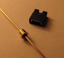
From 1947 to 1960, Esaki joined Kawanishi Corporation (now Denso Ten) and Tokyo Tsushin Kogyo (now Sony). Meanwhile, American physicists John Bardeen, Walter Brattain, and William Shockley invented the transistor, which encouraged Esaki to change fields from vacuum tube to heavily-doped germanium and silicon research in Sony. One year later, he recognized that when the PN junction width of germanium is thinned, the current-voltage characteristic is dominated by the influence of the tunnel effect and, as a result, he discovered that as the voltage is increased, the current decreases inversely, indicating negative resistance. This discovery was the first demonstration of solid tunneling effects in physics, and it was the birth of new electronic devices in electronics called Esaki diode (or tunnel diode). He received a doctorate degree from UTokyo due to this breakthrough invention in 1959.
In 1973, Esaki was awarded the Nobel Prize[3] for research conducted around 1958 regarding electron tunneling[4] in solids. He became the first Nobel laureate to receive the prize from the hands of the King Carl XVI Gustaf.
Semiconductor superlattice
Esaki moved to the United States in 1960 and joined the IBM T. J. Watson Research Center, where he became an IBM Fellow in 1967. He predicted that semiconductor superlattices will be formed to induce a differential negative-resistance effect via an artificially one-dimensional periodic structural changes in semiconductor crystals. His unique "molecular beam epitaxy" thin-film crystal growth method can be regulated quite precisely in ultrahigh vacuum. His first paper on the semiconductor superlattice[5] was published in 1970. A 1987 comment by Esaki regarding the original paper notes:
"The original version of the paper was rejected for publication by Physical Review on the referee's unimaginative assertion that it was 'too speculative' and involved 'no new physics.' However, this proposal was quickly accepted by the Army Research Office..."[6]
In 1972, Esaki realized his concept of superlattices in III-V group semiconductors, later the concept influenced many fields like metals, and magnetic materials. He was awarded the IEEE Medal of Honor "for contributions to and leadership in tunneling, semiconductor superlattices, and quantum wells"[7] in 1991 and the Japan Prize "for the creation and realization of the concept of man-made superlattice crystals which lead to generation of new materials with useful applications" in 1998.[8]
Esaki's “five don’ts” rules
In 1994 Lindau Nobel Laureate Meetings, Esaki suggests a list of “five don’ts” which anyone in realizing his creative potential should follow. Two months later, the chairman of the Nobel Committee for Physics Carl Nordling incorporated the rules in his own speech.[9][2]
- Don't allow yourself to be trapped by your past experiences.
- Don't allow yourself to become overly attached to any one authority in your field – the great professor, perhaps.
- Don't hold on to what you don't need.
- Don't avoid confrontation.
- Don't forget your spirit of childhood curiosity.
Later years
In 1977, Esaki was elected as a member into the National Academy of Engineering for contributions to the engineering of semiconductor devices.
Esaki moved back to Japan in 1992. Subsequently, he served as president of the University of Tsukuba[1] and Shibaura Institute of Technology. Since 2006 he is the president of Yokohama College of Pharmacy. Esaki is also the recipient of The International Center in New York's Award of Excellence, the Order of Culture (1974) and the Grand Cordon of the Order of the Rising Sun (1998).
In recognition of three Nobel laureates' contributions, the bronze statues of Shin'ichirō Tomonaga, Leo Esaki, and Makoto Kobayashi were set up in the Central Park of Azuma 2 in Tsukuba City in 2015.[10]
After the death of Yoichiro Nambu in 2015, Esaki is the eldest Japanese Nobel laureate.
His daughter, Anna Esaki, is married to Craig S. Smith, former Shanghai bureau chief of The New York Times and China bureau chief of The Wall Street Journal .[11]
Recognition
Awards and honors
- 1959 – Nishina Memorial Prize
- 1960 – Asahi Prize
- 1961 – Stuart Ballantine Medal
- 1965 – Japan Academy Prize
- 1973 – Nobel Prize in Physics
- 1974 – Order of Culture
- 1985 – James C. McGroddy Prize for New Materials
- 1989 – Harold Pender Award
- 1991 – IEEE Medal of Honor
- 1998 – Japan Prize
- 1998 – Grand Cordon of the Order of the Rising Sun
- 2001 – Honorary Doctor at the Hong Kong University of Science and Technology
- 2007 – Honorary Distinguished Professor at the National Tsing Hua University
Membership in learned societies
- 1960 Fellow of the American Physical Society
- Physical Society of Japan
- 1975 – Member, the Japan Academy
- 1976 – Foreign Associate, National Academy of Sciences
- 1977 – Foreign Associate, National Academy of Engineering
- 1989 – Member, Max Planck Society
- 1991 – Member, American Philosophical Society
- 1994 – Foreign Member, Russian Academy of Sciences
- 1995 – Honorary Foreign Member, Korean Academy of Science and Technology
- 1996 – Member, Accademia dei Lincei
See also
- List of Japanese Nobel laureates
- List of Nobel laureates affiliated with the University of Tokyo
References
- ↑ 1.0 1.1 1.2 1.3 Dr. Leo Esaki. japanprize.jp
- ↑ 2.0 2.1 江崎玲於奈『限界への挑戦―私の履歴書』(日本経済新聞出版社)2007年
- ↑ Esaki, Leo, "Long Journey into Tunneling," Nobel Lecture, December 12, 1973.
- ↑ Esaki, L. (1958). "New Phenomenon in Narrow Germanium p-n Junctions". Physical Review 109 (2): 603. doi:10.1103/PhysRev.109.603. Bibcode: 1958PhRv..109..603E.
- ↑ Esaki, L.; Tsu, R. (1970). "Superlattice and Negative Differential Conductivity in Semiconductors". IBM Journal of Research and Development 14: 61–65. doi:10.1147/rd.141.0061.
- ↑ "This Weeks's Citation Classic", Current Contents No 28, July 13, 1987.
- ↑ "IEEE Medal of Honor Recipients". April 22, 2015. http://www.ieee.org/documents/moh_rl.pdf.
- ↑ 8.0 8.1 "The Japan Prize Foundation". https://www.japanprize.jp/en/prize_prof_1998_esaki.html.
- ↑ Nordling, Carl (1995). "How to get the Nobel Prize in physics". Physica Scripta 59: 21–25. doi:10.1088/0031-8949/1995/T59/001. Bibcode: 1995PhST...59...21N. https://web.stanford.edu/~rotundu/documents/how_to_get_it.pdf.
- ↑ "ノーベル賞:江崎、小林、朝永氏の銅像やレリーフ設置 完成記念式でお披露目 「子どもが夢を」−−つくば・中央公園 /茨城 - 毎日新聞". http://mainichi.jp/feature/news/m20150316ddlk08040111000c.html.
- ↑ "Anna Esaki Wed To Craig S. Smith" (in en-US). The New York Times. 1990-01-14. ISSN 0362-4331. https://www.nytimes.com/1990/01/14/style/anna-esaki-wed-to-craig-s-smith.html.
Further reading
- Large scale integrated circuits technology: state of the art and prospects, proceedings of the NATO Advanced Study Institute on "Large Scale Integrated Circuits Technology: State of the Art and Prospects," Erice, Italy, July 15–27, 1981 / edited by Leo Esaki and Giovanni Soncini (1982)
- Highlights in condensed matter physics and future prospects / edited by Leo Esaki (1991)
External links
- Miss nobel-id as parameter including the Nobel Lecture, December 12, 1973 Long Journey into Tunnelling
- IBM record
- IEEE History Center – Leo Esaki. Retrieved July 19, 2011 from Leo Esaki - Engineering and Technology History Wiki
- Sony History – The Esaki Diode. Retrieved August 5, 2003 from Sony Global | Sony History
- Freeview video 'An Interview with Leo Esaki' by the Vega Science Trust
 |


