Chemistry:Tungsten disulfide

| |
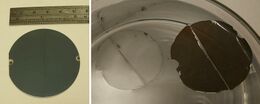
 Left: WS2 film on sapphire. Right: dark exfoliated WS2 film floating on water
| |
| Names | |
|---|---|
| IUPAC names
Tungsten sulfur
Bis(sulfanylidene)tungsten | |
| Systematic IUPAC name
Dithioxotungsten | |
| Other names
Tungsten(IV) sulfide
Tungstenite | |
| Identifiers | |
3D model (JSmol)
|
|
| ChEBI | |
| ChemSpider | |
| EC Number |
|
PubChem CID
|
|
| |
| |
| Properties | |
| WS2 | |
| Molar mass | 247.98 g/mol |
| Appearance | Blue-gray powder[1] |
| Density | 7.5 g/cm3, solid[1] |
| Melting point | 1,250 °C (2,280 °F; 1,520 K) decomposes[1] |
| Slightly soluble | |
| Band gap | ~1.35 eV (optical, indirect, bulk)[2][3] ~2.05 eV (optical, direct, monolayer)[4] |
| +5850·10−6 cm3/mol[5] | |
| Structure | |
| Molybdenite | |
| Trigonal prismatic (WIV) Pyramidal (S2−) | |
| Related compounds | |
Other anions
|
Tungsten(IV) oxide Tungsten diselenide Tungsten ditelluride |
Other cations
|
Molybdenum disulfide Tantalum disulfide Rhenium disulfide |
Except where otherwise noted, data are given for materials in their standard state (at 25 °C [77 °F], 100 kPa). | |
| Infobox references | |
Tungsten disulfide is an inorganic chemical compound composed of tungsten and sulfur with the chemical formula WS2. This compound is part of the group of materials called the transition metal dichalcogenides. It occurs naturally as the rare mineral tungstenite. This material is a component of certain catalysts used for hydrodesulfurization and hydrodenitrification.
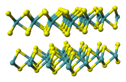
WS2 adopts a layered structure similar, or isotypic with MoS2, instead with W atoms situated in trigonal prismatic coordination sphere (in place of Mo atoms). Owing to this layered structure, WS2 forms non-carbon nanotubes, which were discovered after heating a thin sample of WS2 in 1992.[6]
Structure and physical properties

Bulk WS2 forms dark gray hexagonal crystals with a layered structure. Like the closely related MoS2, it exhibits properties of a dry lubricant.
Although it has long been thought that WS2 is relatively stable in ambient air, recent reports on the ambient air oxidation of monolayer WS2 have found this to not be the case. In the monolayer form, WS2 is converted rather rapidly (over the course of days in ambient light and atmosphere) to tungsten oxide via a photo-oxidation reaction involving visible wavelengths of light readily absorbed by monolayer WS2 (< ~660 nm; > ~1.88 eV).[8] In addition to light of suitable wavelength, the reaction likely requires both oxygen and water to proceed, with the water thought to act as a catalyst for oxidation. The products of the reaction likely include various tungsten oxide species and sulfuric acid. The oxidation of other semiconductor transition metal dichalcogenides (S-TMDs) such as MoS2, has similarly been observed to occur in ambient light and atmospheric conditions.[9]
WS2 is also attacked by a mixture of nitric and hydrofluoric acid. When heated in oxygen-containing atmosphere, WS2 converts to tungsten trioxide. When heated in absence of oxygen, WS2 does not melt but decomposes to tungsten and sulfur, but only at 1250 °C.[1]
Historically monolayer WS2 was isolated using chemical exfoliation via intercalation with lithium from n-butyl lithium (in hexane), followed by exfoliation of the Li intercalated compound by sonication in water.[10] WS2 also undergoes exfoliation by treatment with various reagents such as chlorosulfonic acid[11] and the lithium halides.[12]
Synthesis
WS2 is produced by a number of methods.[1][13] Many of these methods involve treating oxides with sources of sulfide or hydrosulfide, supplied as hydrogen sulfide or generated in situ.
Thin films and monolayers
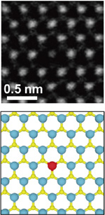
Widely used techniques for the growth of monolayer WS2 include chemical vapor deposition (CVD), physical vapor deposition (PVD) or metal organic chemical vapor deposition (MOCVD), though most current methods produce sulfur vacancy defects in excess of 1×1013 cm−2.[14] Other routes entail thermolysis of tungsten(VI) sulfides (e.g., (R4N)2WS4) or the equivalent (e.g., WS3).[13]
Freestanding WS2 films can be produced as follows. WS2 is deposited on a hydrophilic substrate, such as sapphire, and then coated with a polymer, such as polystyrene. After dipping the sample in water for a few minutes, the hydrophobic WS2 film spontaneously peels off.[15]
Applications
WS2 is used, in conjunction with other materials, as catalyst for hydrotreating of crude oil.[13] In recent years it has also found applications as a saturable for passively mode locked fibre lasers resulting in femtosecond pulses being produced.
Lamellar tungsten disulphide is used as a dry lubricant for fasteners, bearings, and molds,[16] as well as having significant use in aerospace and military industries.[17][failed verification] WS2 can be applied to a metal surface without binders or curing, via high-velocity air impingement. The most recent official standard for this process is laid out in the SAE International specification AMS2530A.[18]
Research
Like MoS2, nanostructured WS2 is actively studied for potential applications, such as storage of hydrogen and lithium.[11] WS2 also catalyses hydrogenation of carbon dioxide:[11][19][20]
- CO2 + H2 → CO + H2O
Nanotubes
Tungsten disulfide is the first material which was found to form non-carbon nanotubes, in 1992.[6] This ability is related to the layered structure of WS2, and macroscopic amounts of WS2 have been produced by the methods mentioned above.[13] WS2 nanotubes have been investigated as reinforcing agents to improve the mechanical properties of polymeric nanocomposites. In a study, WS2 nanotubes reinforced biodegradable polymeric nanocomposites of polypropylene fumarate (PPF) showed significant increases in the Young's modulus, compression yield strength, flexural modulus and flexural yield strength, compared to single- and multi-walled carbon nanotubes reinforced PPF nanocomposites, suggesting that WS2 nanotubes may be better reinforcing agents than carbon nanotubes.[21] The addition of WS2 nanotubes to epoxy resin improved adhesion, fracture toughness and strain energy release rate. The wear of the nanotubes-reinforced epoxy is lower than that of pure epoxy.[22] WS2 nanotubes were embedded into a poly(methyl methacrylate) (PMMA) nanofiber matrix via electrospinning. The nanotubes were well dispersed and aligned along fiber axis. The enhanced stiffness and toughness of PMMA fiber meshes by means of non-carbon nanotubes addition may have potential uses as impact-absorbing materials, e.g. for ballistic vests.[23][24]
WS2 nanotubes are hollow and can be filled with another material, to preserve or guide it to a desired location, or to generate new properties in the filler material which is confined within a nanometer-scale diameter. To this goal, non-carbon nanotube hybrids were made by filling WS2 nanotubes with molten lead, antimony or bismuth iodide salt by a capillary wetting process, resulting in PbI2@WS2, SbI3@WS2 or BiI3@WS2 core–shell nanotubes.[25]
Nanosheets
WS2 can also exist in the form of atomically thin sheets.[26] Such materials exhibit room-temperature photoluminescence in the monolayer limit.[27]
Transistors
Taiwan Semiconductor Manufacturing Company (TSMC) is investigating use of WS2 as a channel material in field effect transistors. The approximately 6-layer thick material is created using chemical vapor deposition (CVD).[28]
References
- ↑ 1.0 1.1 1.2 1.3 1.4 Eagleson, Mary (1994). Concise encyclopedia chemistry. Walter de Gruyter. p. 1129. ISBN 978-3-11-011451-5. https://books.google.com/books?id=Owuv-c9L_IMC&pg=PA1129.
- ↑ Kam, K. K.; Parkinson, B. A. (February 1982). "Detailed photocurrent spectroscopy of the semiconducting group VIB transition metal dichalcogenides". Journal of Physical Chemistry 86 (4): 463–467. doi:10.1021/j100393a010.
- ↑ Baglio, Joseph A.; Calabrese, Gary S.; Kamieniecki, Emil; Kershaw, Robert; Kubiak, Clifford P.; Ricco, Antonio J.; Wold, Aaron; Wrighton, Mark S. et al. (July 1982). "Characterization of n‐Type Semiconducting Tungsten Disulfide Photoanodes in Aqueous and Nonaqueous Electrolyte Solutions Photo‐oxidation of Halides with High Efficiency". J. Electrochem. Soc. 129 (7): 1461–1472. doi:10.1149/1.2124184. Bibcode: 1982JElS..129.1461B.
- ↑ Gutiérrez, Humberto; Perea-López, Nestor; Elías, Ana Laura; Berkdemir, Ayse; Wang, Bei; Lv, Ruitao; López-Urías, Florentino; Crespi, Vincent H. et al. (November 2012). "Extraordinary Room-Temperature Photoluminescence in Triangular WS2 Monolayers". Nano Letters 13 (8): 3447–3454. doi:10.1021/nl3026357. PMID 23194096. Bibcode: 2013NanoL..13.3447G.
- ↑ Haynes, William M., ed (2011). CRC Handbook of Chemistry and Physics (92nd ed.). Boca Raton, FL: CRC Press. p. 4.136. ISBN 1439855110.
- ↑ 6.0 6.1 "Polyhedral and cylindrical structures of tungsten disulphide". Nature 360 (6403): 444–446. 1992. doi:10.1038/360444a0. Bibcode: 1992Natur.360..444T.
- ↑ Sasaki, Shogo; Kobayashi, Yu; Liu, Zheng; Suenaga, Kazutomo; Maniwa, Yutaka; Miyauchi, Yuhei; Miyata, Yasumitsu (2016). "Growth and optical properties of Nb-doped WS2 monolayers". Applied Physics Express 9 (7): 071201. doi:10.7567/APEX.9.071201. Bibcode: 2016APExp...9g1201S.

- ↑ Kotsakidis, Jimmy C.; Zhang, Qianhui; Vazquez de Parga, Amadeo L.; Currie, Marc; Helmerson, Kristian; Gaskill, D. Kurt; Fuhrer, Michael S. (July 2019). "Oxidation of Monolayer WS2 in Ambient Is a Photoinduced Process". Nano Letters 19 (8): 5205–5215. doi:10.1021/acs.nanolett.9b01599. PMID 31287707. Bibcode: 2019NanoL..19.5205K.
- ↑ Gao, Jian; Li, Baichang; Tan, Jiawei; Chow, Phil; Lu, Toh-Ming; Koratker, Nikhil (January 2016). "Aging of Transition Metal Dichalcogenide Monolayers". ACS Nano 10 (2): 2628–2635. doi:10.1021/acsnano.5b07677. PMID 26808328.
- ↑ Joensen, Per; Frindt, R. F.; Morrison, S. Roy (1986). "Single-layer MoS2". Materials Research Bulletin 21 (4): 457–461. doi:10.1016/0025-5408(86)90011-5.
- ↑ 11.0 11.1 11.2 Bhandavat, R.; David, L.; Singh, G. (2012). "Synthesis of Surface-Functionalized WS2 Nanosheets and Performance as Li-Ion Battery Anodes". The Journal of Physical Chemistry Letters 3 (11): 1523–30. doi:10.1021/jz300480w. PMID 26285632.
- ↑ Ghorai, Aru; Midya, Anupam; Maiti, Rishi; Ray, Samit K. (2016). "Exfoliation of WS2 in the semiconducting phase using a group of lithium halides: a new method of Li intercalation". Dalton Transactions 45 (38): 14979–14987. doi:10.1039/C6DT02823C. PMID 27560159.
- ↑ 13.0 13.1 13.2 13.3 Panigrahi, Pravas Kumar; Pathak, Amita (2008). "Microwave-assisted synthesis of WS2 nanowires through tetrathiotungstate precursors" (free download). Sci. Technol. Adv. Mater. 9 (4): 045008. doi:10.1088/1468-6996/9/4/045008. PMID 27878036. Bibcode: 2008STAdM...9d5008P.
- ↑ Hong, Jinhua; Hu, Zhixin; Probert, Matt; Li, Kun; Lv, Danhui; Yang, Xinan; Gu, Lin; Mao, Nannan et al. (February 2015). "Eploring atomic defects in molybdenum disulphide monolayers". Nature Communications 6: 6293. doi:10.1038/ncomms7293. PMID 25695374. Bibcode: 2015NatCo...6.6293H.
- ↑ Yu, Yang; Fong, Patrick W. K.; Wang, Shifeng; Surya, Charles (2016). "Fabrication of WS2/GaN p-n Junction by Wafer-Scale WS2 Thin Film Transfer". Scientific Reports 6: 37833. doi:10.1038/srep37833. PMID 27897210. Bibcode: 2016NatSR...637833Y.
- ↑ "Dicronite". Machinery (Machinery Publications Corporation) 73: 101. 1967. https://books.google.com/books?id=7rYiAQAAMAAJ&q=dicronite.
- ↑ "Quality Approved Special Processes By Special Process Code". BAE Systems. 2020-07-07. https://www.baesystems.com/en-us/our-company/inc-businesses/electronic-systems/supplier-center.
- ↑ "AMS2530A: Tungsten Disulfide Coating, Thin Lubricating Film, Binder-Less Impingement Applied". SAE International. https://www.sae.org/standards/content/ams2530a/.
- ↑ Lassner, Erik; Schubert, Wolf-Dieter (1999). Tungsten: properties, chemistry, technology of the element, alloys, and chemical compounds. Springer. pp. 374–. ISBN 978-0-306-45053-2. https://books.google.com/books?id=foLRISkt9gcC&pg=PA374.
- ↑ Engineer making rechargeable batteries with layered nanomaterials. Science Daily (2013-01-016)
- ↑ Lalwani, Gaurav (September 2013). "Tungsten disulfide nanotubes reinforced biodegradable polymers for bone tissue engineering". Acta Biomaterialia 9 (9): 8365–8373. doi:10.1016/j.actbio.2013.05.018. PMID 23727293.
- ↑ Zohar, E. (2011). "The Mechanical and Tribological Properties of Epoxy Nanocomposites with WS2 Nanotubes". Sensors & Transducers Journal 12 (Special Issue): 53–65. http://www.sensorsportal.com/HTML/DIGEST/P_SI_159.htm.
- ↑ Reddy, C. S.; Zak, A.; Zussman, E. (2011). "WS2 nanotubes embedded in PMMA nanofibers as energy absorptive material". J. Mater. Chem. 21 (40): 16086–16093. doi:10.1039/C1JM12700D.
- ↑ Nano-Armor: Protecting the Soldiers of Tomorrow. Physorg.com (2005-12-10). Retrieved on 2016-01-20
- ↑ Kreizman, Ronen; Enyashin, Andrey N.; Deepak, Francis Leonard; Albu-Yaron, Ana; Popovitz-Biro, Ronit; Seifert, Gotthard; Tenne, Reshef (2010). "Synthesis of Core-Shell Inorganic Nanotubes". Adv. Funct. Mater. 20 (15): 2459–2468. doi:10.1002/adfm.201000490.
- ↑ Coleman, J. N.; Lotya, M.; O'Neill, A.; Bergin, S. D.; King, P. J.; Khan, U.; Young, K.; Gaucher, A. et al. (2011). "Two-Dimensional Nanosheets Produced by Liquid Exfoliation of Layered Materials". Science 331 (6017): 568–71. doi:10.1126/science.1194975. PMID 21292974. Bibcode: 2011Sci...331..568C. https://www.researchgate.net/publication/49809453.
- ↑ Gutiérrez, Humberto R.; Perea-López, Nestor; Elías, Ana Laura; Berkdemir, Ayse; Wang, Bei; Lv, Ruitao; López-Urías, Florentino; Crespi, Vincent H. et al. (2013). "Extraordinary Room-Temperature Photoluminescence in Triangular WS2 Monolayers". Nano Letters 13 (8): 3447–54. doi:10.1021/nl3026357. PMID 23194096. Bibcode: 2013NanoL..13.3447G.
- ↑ Cheng, Chao-Ching; Chung, Yun-Yan; Li, Uing-Yang; Lin, Chao-Ting; Li, Chi-Feng; Chen, Jyun-Hong; Lai, Tung-Yen; Li, Kai-Shin et al. (2019). "First demonstration of 40-nm channel length top-gate WS2 pFET using channel area-selective CVD growth directly on SiOx/Si substrate". 2019 Symposium on VLSI Technology. IEEE. pp. T244–T245. doi:10.23919/VLSIT.2019.8776498. ISBN 978-4-86348-719-2.
 |

